Early Stage of Polycrystalleve Growth of Ge and SiGe by Reactive Thermal CVD from GeF 4 and Si 2 H 6
- PDF / 1,619,813 Bytes
- 5 Pages / 414.72 x 648 pts Page_size
- 15 Downloads / 330 Views
JUN-ICHI HANNA, TAKAYUKI OHUCHI AND MASAJI YAMAMOTO Tokyo Institute of Technology, Imaging Science & Engineering Lab., Yokohama 226, Japan
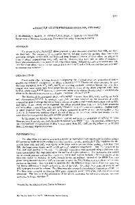
ABSTRACT We have investigated the structure and crystallinity of poly SiGe and Ge films in the early stage of their growth prepared at 500'C.6) from Si2 -6 and GeH4. The present technique, however, provides us crystalline SiGe and Ge films even at 350-400°C ("low-temperature regime"), where selective epitaxy takes place on the Si02-patterned Si substrate 7"8). A specific condition for polycrystalline growth in this CVD, i.e., at >4000 C ("high temperature regime"), where polycrystalline SiGe and Ge films were non-selectively grown regardless of substrate materials, was selected for the present study. Their growth rates were around -lnm/sec. Fig. I shows a cross sectional SEM micrograph of a typical poly- SiGe film whose thickness is about 400nm. No fine structure is seen in the micrograph except the disdistinctive surface morphology, which is probably due to the island growth of film on the substrate, in contrast to the columnar structures which are often encountered in the low-temperature CVD films of poly Si. The film exhibited a preferential orientation to the (220) plane in the XRD spectra and displayed high crystallinity, judging from the narrow FWHM of the Raman peak at 300cm"' for a TO mode of Ge-Ge bonds in the crystal. The incorporation of Si into the film, which became obvious at higher gas flow ratios, (Si2H6 /GeF4 over 10), did not degrade the crystallinity of the film by making it amorphous, at least up to 60% at least.
Fig. I SEM micrograph of typical poly-
SiGe film
EMUg
.
.
.
.
.
0
Si0 2(TEOS)
0
Si0 2(Thermal oxidized) //0
10001-
.
800 F
.1
... /0
600 I
/
S/
E 400
I
LI.°
200
0
I
0
5
10
15
20
Growth Time (min)
Film structure in the early stage of the growth
Fig. 2 Film thickness as a function of growth time 879
The film growth exhibited a certain induction time when deposited on the Si02 surface, as is shown in Fig.2, in which the film thickness is plotted as a function of the deposition time. The thickness increased linearly with increasing the deposition time after the induction time. The averaged growth rate was 9.6 A/sec in these films. The crystallinity of these films were studied by Raman spectroscopy, as shown in Fig.3. The peak at 300 cm" in the Raman spectrum took shape clearly even in the thin film whose thickness was as thin as
Data Loading...