Effect Of AlGaN/GaN Strained Layer Superlattice Period On InGaN MQW Laser Diodes
- PDF / 542,387 Bytes
- 6 Pages / 612 x 792 pts (letter) Page_size
- 50 Downloads / 314 Views
INTRODUCTION GaN based laser diodes have potential in a number of applications such as optical data storage, printing, full-color displays and chemical sensors. Additionally, medical applications of nitride based lasers include laser ablation of tissue (e.g. angioplasty), optical detection and selective destruction of malignant tumors, and autoflourescence imaging for the early detection of cancer. Major developments in recent years have led to lifetimes in excess of 10,000 hours demonstrating the viability of nitride laser diodes for commercial applications [1]. Superlattices have been studied in the cladding for two reasons. First, it is difficult to grow thick AlGaN cladding layers needed for optical confinement due to cracking from lattice mismatch stresses during growth. AlGaN/GaN strained layer superlattices (SLSs) have been employed for strain relief of the cladding layer [2,3]. Secondly, Mgdoped AlGaN/GaN superlattices have also shown an enhanced hole concentration. Kozodoy et al. show that a periodic oscillation of the valence band edge, such as superlattices employing alloys with different valence band edge positions, can help overcome the poor doping efficiency of a deep acceptor by forming a two-dimensional hole gas (2DHG) [4]. This results from the ionization of acceptors when the band edge is far below the Fermi energy causing an accumulation of holes where the band edge is close to the Fermi level. Although the free carriers are separated into parallel sheets, their overall number may be much higher than in a simple bulk film. The average hole concentration of superlattice layers at room temperature increases by more than a factor
F99W1.4
Downloaded from https://www.cambridge.org/core. Uppsala Universitetsbibliotek, on 22 May 2020 at 07:29:24, subject to the Cambridge Core terms of use, available at https://www.cambridge.org/core/terms. https://doi.org/10.1557/S1092578300004026
of 10 over bulk films. This paper investigates the effect of vertical conduction of AlGaN/GaN superlattice cladding layers on InGaN laser diode structures.
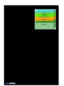
EXPERIMENTAL DETAILS InGaN multi-quantum well laser diodes were grown by metalorganic chemical vapor deposition (MOCVD) in a two-flow horizontal reactor on c-plane sapphire substrates using both atmospheric and low pressure. The device structure shown in Figure 1 has an active region consisting of a 3 period In0.15Ga0.85N (40 Å)/In0.05Ga0.95N:Si (85Å) MQW with a 200 Å Al0.2Ga0.8N:Mg cap. The n- and p-type cladding regions surrounding the active region consisted of Al0.2Ga0.8N/GaN superlattices with a total thickness of 0.5 µm. The cladding regions were Si doped for the n-cladding and Mg doped for the p-cladding. The laser structures were grown with superlattice periods of 40 Å, 55 Å, 70 Å, 80 Å, 100 Å, 110 Å and 140 Å. The thickness of the AlGaN and GaN layers were the same yielding an average composition of 10% Al in the cladding. One structure was grown with a 0.5 µm thick bulk Al0.1Ga0.9N cladding layer for comparison purposes. A GaN:Mg layer was used for a contact
Data Loading...