Effect of Ammonium Acetate on the Properties of Chemical Bath Deposited CdS Films
- PDF / 3,002,285 Bytes
- 6 Pages / 612 x 792 pts (letter) Page_size
- 96 Downloads / 393 Views
Effect of Ammonium Acetate on the Properties of Chemical Bath Deposited CdS Films Abeer A. Al-Yafeai1, Sovannary Phok1, Sahar A. Al-Shaibani1, Shifaa M. Al-Baity1, Esmaeel M. Al-Hammadi1 and Falah S. Hasoon1 1
National Energy and Water Research Center, Abu Dhabi Water and Electricity Authority, P.O.
Box 54111, Abu Dhabi, United Arab Emirates.
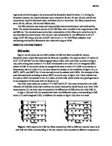
ABSTRACT This investigation is a comprehensive study of the effect of ammonium acetate on the electrical, optical, morphology and microstructure of CdS thin films grown by Chemical Bath Deposition method (CBD). Two sets of CdS thin films (A and B) were deposited on glass substrates at 60°C for 60 min. The films were deposited using chemical bath solution that consists of cadmium acetate, ammonium hydroxide, and thiourea. However, ammonium acetate was added into the chemical bath used to deposit set (B), where ammonium acetate was eliminated from bath solution used to deposit set (A). The films’ morphology was examined by Field Emission Scanning Electron Microscopy (FE-SEM), whereas, the chemical composition was investigated by Electron Probe Micro-Analyzer (EPMA). The X-Ray Diffraction (XRD) θ/2θ technique was applied to study the structure of the films. Atomic Force Microscopy (AFM) was used to measure the average surface roughness of the films, and Dektak Profilometer was used to determine the CdS films thickness. The optical and electrical properties for the films were determined using UV-Vis-NIR Spectrometer, and the Hall Effect technique, respectively. The highest carrier mobility was obtained for the films deposited in an ammonium acetate free bath. However, both films were polycrystalline with hexagonal structure exhibiting a tendency toward texture, that increase with increasing the pH value of the chemical bath. INTRODUCTION Cadmium sulfide (CdS) thin films play an important role in the development of costeffective and reliable photovoltaic devices. CdS thin films have been used as junction partners in CdTe and CIGS solar cells for many years. This is due to its suitable band gap, high transmittance and low resistivity [1-4]. Several methods have been used to prepare CdS thin films: vacuum evaporation [ 5], sputtering [6], electrodeposition [7], molecular beam epitaxy (MBE) [ 8, 9], screen printing [10], metal organic chemical vapor deposition (MOCVD) [11, 12], pulsed laser ablation [13], close-space sublimation (CSS) [14], spray pyrolysis [15], and chemical bath deposition (CBD) [1-4, 16-23]. The best device performance has been achieved using a CdS buffer layer grown by CBD method. The highest efficiency currently reported for both CIGS and CdTe thin film solar cells is 19.6 % [16]. CBD is a simple, low cost, and flexible method that can be used to deposit CdS thin films on different types, shapes and sizes of substrates [17]. Also it is a convenient method that can be applied in an industrial scale [17, 18]. The physical properties and the deposition rate of the CdS films depend on different growth parameters such as the bath temperature, the relative concentrati
Data Loading...