Effect of barrier layers on the texture and microstructure of Copper films
- PDF / 1,344,773 Bytes
- 6 Pages / 612 x 792 pts (letter) Page_size
- 85 Downloads / 330 Views
E2.2.1
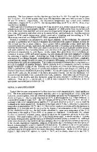
Effect of barrier layers on the texture and microstructure of Copper films Tejodher Muppidi and David P Field School of MME, Washington State University, Pullman, WA. John E Sanchez Advanced Micro Devices, Sunnyvale, CA. ABSTRACT: The microstructure of interconnect material is know to influence its electromigration and stress-voiding properties. In addition to many factors responsible for the microstructure development, the barrier layer could be a major contributing factor as it forms the substrate for the copper films above. The microstructure of the barrier films based on its deposition technique could determine the final microstructure of the copper film. In the present work we examine the effect of two different barrier layers (Ta and TaN) and different stackings of these two materials on the microstructure on the copper seed (PVD) and electroplated films using EBSD, AFM and XRD. The results show that the plated films have a predominantly (111) texture and uniform grain size. But the (111) texture maximum varied with the barrier layer stacking underneath the plated film.
INTRODUCTION: Copper is fast replacing aluminum as the material in interconnects1. The lower resistivity of copper in addition to its better performance with respect to electromigration and stress-voiding are the important factors influencing this change. But, the major problem in using copper comes from its poor diffusion properties in dielectrics. Copper diffuses easily in to the dielectric thereby poisoning the device. Copper also has poor adhesion to the dielectric. These problems are overcome by use of a barrier layer which prevents the diffusion of Cu into the dielectric2. Also, the barrier material has better adhesion to both the dielectric and the copper thereby solving the problem of adhesion. The most commonly used dielectric materials are Ta, TaN, W, TiW, W, TiN, etc. Barrier layer materials are usually refractory materials which have high stability at high temperatures (600ºC) and good diffusion resistance3. They are inert and do not cause poisoning of the devices by diffusing in to the dielectrics. Most of the currently used barrier layers are deposited by sputtering5,6 (PVD). But the damascene process for the copper interconnects requires the deposition of the materials in to trenches of varying aspect ratios. So, other techniques like Atomic Layer Deposition10 (ALD) and Chemical vapor deposition (CVD) are being tested for deposition of Ta, TaN and W to achieve better step coverage and better filling. In addition, a combination of layers of these materials has been used as barrier layer eg. Stacking of Ti/TiN, Ta/TaN. All of these have could have an effect on the microstructure of the over layers and hence an impact on the electromigration performance of the interconnects.
Downloaded from https://www.cambridge.org/core. Cornell University Library, on 26 Aug 2020 at 03:00:56, subject to the Cambridge Core terms of use, available at https://www.cambridge.org/core/terms. https://doi.org/10.1557/PROC-766-E2.2
E2.2.2
The c
Data Loading...