Effect of Buffer Electrodes in Crystallization of Zinc Oxide Thin Film for Thin Film Bulk Acoustic Wave Resonator
- PDF / 1,182,862 Bytes
- 6 Pages / 411.12 x 635.4 pts Page_size
- 85 Downloads / 366 Views
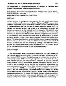
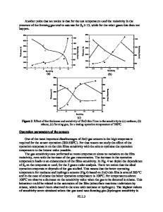
shows the schematic structure of the TBAR. The diaphragm structure is made by a wet etching process of Si (100) wafer. The diaphragm is made of a ZnO piezoelectric thin film sandwiched by upper and lower electrodes on a SiO2 membrane. The diaphragm size is 360 g rmsquare. The SiO 2 membrane is formed by a radio frequency (rf) sputtering on thermally oxidized SiC 2, because about 6.7 pm thickness of SiO2 is needed in this experiment to make an approximately 200MHz TBAR1 The ZnO piezoelectric thin film with a thickness of7.7 p m on the lower electrode is also made by if sputtering. Both the thickness of ZnO and that of SiO2 are designed to cancel the temperature characteristics of frequency of the resonator. Figure 2 shows a schematic figure of the rf sputtering apparatus used in this experiment [11]. Substrates fixed by dome shape holders in a process known as planetary motion were revolved and rotated over the ZnO target to obtain thickness uniformity and stress relaxation [12, 13]. The optimum conditions for making a c-axis oriented ZnO thin film are shown in Table I. Both the lower electrode and the upper electrode are made of Au with a thickness of 200nm, because ZnO on Au shows good c-axis orientation [14]. In this experiment we focused buffer metals under the Au lower electrode to improve the crystallinity of the Au electrode and obtain good crystallinity ZnO thin film. Each NiCr (Ni=80%, Cr=200/o), Ti and Cr, whose thickness is 20nm, is used as a buffer layer ofthe lower electrode, because they maintain good adhesive strength between Au and the substrate. Au, NiCr, Ti and Cr electrodes are formed by electron beam vapor deposition. Substrate
W A
...............
.....
I
7771:.
ZnO
Lowerelectrde
......
I
Upperelecixle
Gas
F 1Sc
aiO, Figure 1 Schematic structure of TBAR-
RF Power
Figure 2 Schematic figure ofthe rf sputtering apparatus.
Table I Optimum conditions for making c-axis-oiented ZnO thin films. Substrate Temperature: Ar/O2gas ratio : Ar/O2 gas pressure: RFpower: Target: Deposition rate;
268
150* C 60/40 1.3 x 101 Pa 13.56MHz ZnO ceramic 0.3 nm/s
RESULTS Figure 3 shows x-ray diffaction (XRD) patterns ofZnO on AWi/SiO, ZnO on Au/NiCr/SiO 2 and ZnO on AuiCr•/S. Each difbi patterm showsacl -axms orientation of ZnO, because only (002) and (004) peaks are som inthe diffiaction chart Figure 4 shows the XRD rncking curves ofZnO on AuTi 7nO on AuNiCr and ZnO on Au/Cr. Figure 5 also shows he XRD rocking curves of Au(1l1) on Ti, Au(l11) on NiCr and
Au(l11) on Cr. Estinating the ful widdh at half maximum (FWIM) of ZnO (002) peaks and Au (111) peaks froin the rocking crves, the FWHM ofZnO (002) on AuTi is 3.78" .It is the smallest of three data, ZnO on AuwTi, ZnO on Au/NiCr and ZnO on Au/Cr, and also Au on Ti shows the smallest FWHM among Au on Ti, Au on NiCr and Au on Cr. These results show dhat well-oriented Au grows on Ti, and well-oiented ZnO grows wel-oriented Au. Thus, it is very inmpomant to select a buffer electrode to form a well-oriented ZnO thin film. Figure 6 shows the relmnh between th
Data Loading...