Effect of Heat Treatment on the Stability of Nanosized (Co 40 Fe 40 B 20 ) 34 (SiO 2 ) 66 /ZnO/In 2 O 3 Multilayers
- PDF / 716,268 Bytes
- 4 Pages / 612 x 792 pts (letter) Page_size
- 35 Downloads / 279 Views
ct of Heat Treatment on the Stability of Nanosized (Co40Fe40B20)34(SiO2)66/ZnO/In2O3 Multilayers I. V. Babkinaa, *, M. N. Volochaevb, O. V. Zhilovaa, Yu. E. Kalinina, M. A. Kashirina, A. V. Sitnikova, M. V. Chehonadskiha, and L. I. Yanchenkoa aVoronezh
State Technical University, Voronezh, 394026 Russia Kirensky Institute of Physics, Krasnoyarsk Scientific Center, Siberian Branch, Russian Academy of Sciences, Krasnoyarsk, 660036 Russia *e-mail: [email protected]
b
Received March 12, 2020; revised April 15, 2020; accepted May 27, 2020
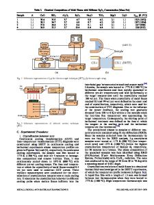
Abstract—An investigation is performed of the thermal stability and phase transformations of thin-film heterogeneous [(Co40Fe40B20)34(SiO2)66/ZnO/In2O3]85 multilayers obtained via ion beam sputtering. The system contains 85 layers, each consisting of a (Co40Fe40B20)34(SiO2)66 composite layer and ZnO and In2O3 semiconductor spacers. The sample structure in the initial state and after heat treatment is studied by means of X-ray diffraction. It is shown that the samples are stable at temperatures of up to 500°С. Zn2SiO4, InBO3, CoFe, and In2O3 phases form during annealing. DOI: 10.3103/S1062873820090051
INTRODUCTION Wide-gap oxide semiconductors are the main functional materials of transparent electronics. It is therefore important to study the solid-state reactions that occur between semiconductor, dielectric, and metal phases in such electronic devices [1–4]. A multilayer film with nanometer thick layers is a model object for observing the formation of compounds at the points of contact between wide-gap oxide semiconductors and metal and dielectric compounds. Earlier studies on solid-phase chemical transformations in the [(Co40Fe40B20)34(SiO2)66/ZnO]112, and [(Co40Fe40B20)34(SiO2)66/SnO2]32, [(Co40Fe40B20)34(SiO2)66/In2O3]92 films showed that the products of reaction depend on the composition and the ratio between the thicknesses of the metal oxide layers and spacers in the composite [5]. On the other hand, different semiconductor compounds can come into contact with metal and dielectric layers in the functional elements of transparent electronics. A Co40Fe40B20 alloy nanograin in our case simultaneously has a common interface with ZnO and In2O3, which can lead to competing transformations during solid-phase chemical reactions. This situation cannot be studied on bilayers. In view of the above, the aim of this work was to establish patterns of the variation in the structure and phase composition of [(Co40Fe40B20)34(SiO2)66/ZnO/In2O3]85 films containing spacers of several semiconductor
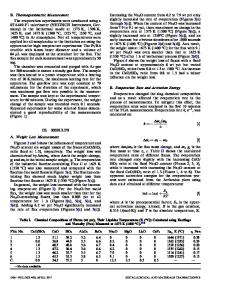
compounds in their initial state and after heat treatment in the temperature range of 200 to 650°С. EXPERIMENTAL [(Co40Fe40B20)34(SiO2)66/ZnO/In2O3]85 multilayer films were obtained via the ion beam sputtering of three targets with layer-by-layer deposition onto the surface of a Si(100) substrate mounted on a rotating carousel, according to the procedure described in [6]. ZnO, In2O3, and Co40Fe40B20 alloy ceramic plates (280 × 80 × 15 mm3 in size) with 13 quartz (SiO2) weights (80 × 10 × 2 mm3 in size)
Data Loading...


