Effect of hydrogen on anisotropy of the p -GaN growth rate in the case of side-wall MOCVD
- PDF / 312,372 Bytes
- 6 Pages / 612 x 792 pts (letter) Page_size
- 64 Downloads / 217 Views
ATION, TREATMENT, AND TESTING OF MATERIALS AND STRUCTURES
Effect of Hydrogen on Anisotropy of the p-GaN Growth Rate in the Case of Side-Wall MOCVD W. V. Lundin^, A. E. Nikolaev, A. V. Sakharov, and A. F. Tsatsul’nikov Ioffe Physicotechnical Institute, Russian Academy of Sciences, St. Petersburg, 194021 Russia ^e-mail: [email protected] Submitted April 23, 2007; accepted for publication May 4, 2007
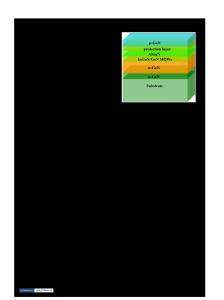
Abstract—The effect of the composition of the carrier gas on anisotropy of p-GaN growth rates in side-wall metal-organic chemical vapor deposition was studied. p-GaN layers with a nominal thickness of ~400 nm were grown on side-walls of GaAs mesa stripes formed preliminarily by selective-area epitaxy on Si3N4. It is shown that, if hydrogen is used as the carrier gas, the p-GaN growth occurs mainly in the lateral direction, so that the p-GaN layer is either absent or is thin at the top faces of mesa stripes; in contrast, if nitrogen is used as the carrier gas, growth in the normal (0001) direction is prevalent, so that a p-GaN layer is formed at all faces of the mesa stripe. The results of our study are indicative of a significant role of hydrogen in the process of epitaxial growth of GaN and can be used in the development of technology of devices with p–n junctions based on GaN and with the use of selective-area growth. PACS numbers: 78.55.Cr, 81.05.Ea, 81.10.Aj, 81.10.Bk, 81.15.Gh, 85.60.Jb DOI: 10.1134/S1063782608020218
1. INTRODUCTION Contemporary methods of epitaxial growth of semiconductor compounds make it possible to grow very complex multilayered structures. However, this undeniable progress was attained at the expense of a “loss of two dimensions.” As a rule, the grown structures are homogeneous in the substrate plane; as a result, formation of a real electronic or optoelectronic device inhomogeneous in all three dimensions is attained in the stages of postgrowth operations (selective etching, doping, formation of insulating regions, and so on). The use of epitaxy inhomogeneous in the substrate plane is restricted to several particular cases, as a rule, related to the formation of passive regions in the devices. At the same time, it seems to be evident that the development of the methods of selective and nonplanar epitaxy for the formation of a real three-dimensional device structure would make it possible to expand significantly the range of potentialities of semiconductor technology. However, development of these methods would require additional study of specific features of the process of epitaxial growth. Epitaxy on nonplanar surfaces is most radically different from planar epitaxy; in the case of nonplanar epitaxy, there is a competition between closely spaced faces with different crystallographic orientations. One of the real applications of the methods of selective epitaxy to the technology of light-emitting devices based on the III–N compounds is related to the growth of LED structures on the side walls of mesa stripes (side-wall epitaxy) [1]. This approach makes it possible to combine the we
Data Loading...