Effect of Si Doping on the Structure of GaN
- PDF / 5,205,697 Bytes
- 7 Pages / 414.72 x 648 pts Page_size
- 67 Downloads / 325 Views
difficulty of achieving useful doping, in particular p-doping in high concentration [3]. High lattice and thermal mismatch between popular substrates such as SiC and sapphire leads to high stress in the layer and eventual layer cracking. To obtain high-brightness blue-light-emitting diodes high reliability and high speed are necessary. High defect density can preclude potential applications. It is not clear at this point how particular doping influences the type of defects and their distribution, and very little is known about how a particular buffer layer helps defect reduction and strain relaxation in the layer. In this paper the influence of Si doping on the structural properties of GaN is described. Undoped and Si doped samples grown by MOCVD with different buffer layers have been studied using transmission electron microscopy (TEM), x-
ray diffraction and Raman spectroscopy. MOCVD GROWN GaN Two sets of GaN layers were grown by MOCVD on sapphire substrates. In one case (1120) A12 0 3 substrates (a plane ) were used for the growth of GaN layers with AIN as a buffer layer. These samples will be called "A." Undoped and Si-doped samples were studied. Undoped samples grown with the low-temperature AIN buffer layer on the cc plane of sapphire were 3.5 gim thick and for Si-doped samples (3x1018 cm- 3 ) were 5 gim thick. The second set of GaN layers were grown on (0001) A12 0 3 substrates using low-temperature GaN as a buffer 487
Mat. Res. Soc. Symp. Proc. Vol. 423 01996 Materials Research Society
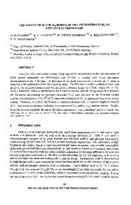
layer. These samples will be called "B." These samples were 1.8 prm thick and all were Si doped with doping levels 9x10 16 cm- 3, 3x10 18 cm-3 and lx1019 cm-3 . X-ray double-crystal diffractometry was used for general characterization of the structural quality of these layers, while TEM techniques were applied for defect investigation. Both plan-view and cross-section specimens were studied by TEM. Raman spectroscopy was used for determination of the strain in the layer. Different amount of broadening of the FWHMs (3.3-8 arc min) of the rocking curves taken for 0-- and 0/20 scans were observed for the "A" samples. More broadening was observed for the undoped samples (Table I). Optical micrographs taken from these two samples show completely different surface roughness. The doped samples had smoother surface. Some large defects could be seen on optical micrographs for both doped and undoped "A" samples. Atomic force microscopy shows that micro-tubes (voids or pin-holes) are formed on the sample surfaces with a diameter of 0.2-0.5 gtm (Fig. la). Some micro-tubes (pinholes or voids) were observed as well, in plan-view TEM samples (Fig. lb). These micro-tubes (about 3 nm diameter) were associated with dislocations with edge components. It is not clear at this point if larger pin-holes observed by AFM have the same nature as these seen in our plan-view samples, since the size of larger pinholes (0.2-0.5 gtm) and distribution practically precludes their observation in high resolution.
aa
4
4
...
Fig. 1. (a) AFM image of a
Data Loading...