Effect of Stresses in Molybdenum Back Contact Film on Properties of CIGSS Absorber Layer
- PDF / 357,629 Bytes
- 7 Pages / 612 x 792 pts (letter) Page_size
- 94 Downloads / 277 Views
F14.13.1
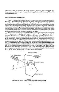
Effect of Stresses in Molybdenum Back Contact Film on Properties of CIGSS Absorber Layer Ankur A. Kadam, Anant H. Jahagirdar and Neelkanth G. Dhere Florida Solar Energy Center, University of Central Florida 1679, Clearlake Road, Cocoa, FL-32922 Tel. (321) 638-1000 x 1230, FAX (321) 638-1010, e-mail: [email protected] ABSTRACT Analysis of CuIn1-xGaxSe2-ySy (CIGSS) absorber and molybdenum back contact layer was carried out to understand the changes in the microstructure of CIGSS layer as a function of the deposition conditions and the nature of stress in the underlying Mo film. All the depositions were carried out on 10 cm x 10 cm glass substrates. Compressive and tensile stressed molybdenum films were prepared with combinations of deposition parameters; power and pressure. CIGSS absorber layer was prepared by depositing metallic precursors using DC magnetron sputtering followed by selenization and sulfurization. Molybdenum layer deposited at 300 W and 3 x 10⁻⁴ Torr pressure produced compressive stress with compact, well adherent and lower sheet resistance as compared to the tensile stressed film deposited at 200 W and 5 x 10⁻³ Torr. The crystallinity of the CIGSS film was found not to depend on the stress in the underlying molybdenum film. However, the adhesion at the Mo/CIGSS as well as gallium profile at the Mo/CIGSS interface were affected by the stress. INTRODUCTION Molybdenum is one of the most important materials used as a back ohmic contact for CIGSS absorber thin-film solar cells because of its high melting temperature and low contact resistance [1, 2]. Generally molybdenum is deposited in two layer sequence to build the requisite thickness. While depositing molybdenum back contact layer on glass and stainless steel substrates, it was observed that the film peeled off and curled from substrate / Mo interface. The goal of the work was to reduce the stress in the Mo film that was relieved during the consequent CIGSS absorber layer preparation. From an electrical point of view, one desires the lowest sheet resistance possible for the back contact of a solar cell, minimizing its contribution to the series resistance of the cell. There is a strong correlation between the energy of the sputtered molybdenum atoms and the working gas sputtering pressure, discharge voltage, and the mass ratio of target and projectile atoms. As a result, significant changes may be induced in the properties of the growing films. At relatively high power and low pressure, the growing films experience compressive stress with dense microstructure due to the high kinetic energy of the arriving atoms. At relatively high sputtering pressures, the energy provided to the growing film is low and consequently films exhibit tensile stress with open porous microstructure [3,4,5]. One mechanism for compressive stress is the atomic peening action that leads to lattice expansion in the growing films induced by incorporated energetic working Ar gas that bombards the growing molybdenum films [6, 7]. CIGSS is one of the most promising absorbe
Data Loading...