Effect of the Bottom Electrode Contact (BEC) on the phase transformation of N 2 doped Ge 2 Sb 2 Te 5 (N-GST) in a Phase-
- PDF / 229,445 Bytes
- 6 Pages / 612 x 792 pts (letter) Page_size
- 100 Downloads / 267 Views
D7.9.1
Effect of the Bottom Electrode Contact (BEC) on the phase transformation of N2 doped Ge2Sb2Te5 (N-GST) in a Phase-change Random Access Memory Suyoun Lee1,*, Y. J. Song1, Y. N. Hwang1, S. H. Lee1, J. H. Park1, K. C. Ryoo1, S. J. Ahn1, C. W. Jeong1, J. H. Oh1, J. M. Shin1, F. Yeung1, W. C. Jeong1, Y. T. Kim2, J. B. Park3, K. H. Koh1, G. T. Jeong1, H. S. Jeong1 and Kinam Kim1 1 Advanced Technology Development Team, Samsung Electronics, Yongin-City, South Korea; 2 CAE Team, Samsung Electronics Co.,Ltd, Yongin-City, South Korea; 3 AE Lab, Samsung Advanced Institute of Technology, Yongin-City, South Korea. With respect to the operation of a Phase-change Random Access Memory (PRAM or PcRAM), we studied the effect of the contact between the electrode metal and the chalcogenide glass, N2 doped Ge2Sb2Te5 in this report. We investigated a change of the resistance-programming current pulse (R-I) curve varying the contact size and the electrode material. Also we tested the surface oxidation of the electrode. We found that the programming current, the resistance of the programmed state (“RESET”) and the erased state (“SET”) were highly dependent on the above parameters. These results are presented and a more effective way to the high density PRAM will be proposed. I. Introduction Recent great development of information technology, gradually but strongly, demands new memory devices with outstanding memory properties such as the nonvolatility, high speed, good scalibility, and strong radiation hardness. Among them, phase-change random access memory (PRAM), based on the difference of resistance from the phase transition of an amorphous chalcogenide glass [1], is attracting enormous interest because of its good scalibility, simple structure, and low process cost [2]. Hence, there have been numerous approaches and challenging issues for realizing the conceptual device into mass-productive memory products. In particular, one of the major obstacles for commercial high density PRAM is too large cell current (RESET current, IRESET) required for melting the programmed region of the chalcogenide glass for amorphous phase of “RESET” state. Therefore, it is highly required to reduce the IRESET to the low level, which can be supplied by very small CMOS transistors. In addition to the reduction of reset current, it is very important to maintain a low set resistance, because the set resistance is typically increased in the decrease of reset current, resulting in deteriorating a sensing margin of the device. There are several processing parameters to determine the reset current and set resistance. In various experiments, it was found that bottom electrode has a critical effect on IRESET and RSET. Unfortunately, there are few studies on the effect of bottom electrode on IRESET. In this paper, we investigate and evaluate the correlation of IRESET and RSET
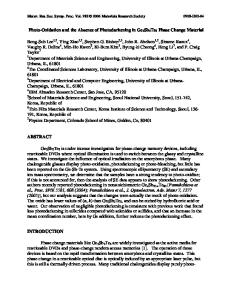
D7.9.2
(a) (b) Fig. 1. (a) A vertical TEM image of a fabricated PCRAM cell and (b) a storage module. with the contact size, the electrical resistivity, and the surface treatment of the
Data Loading...