Effects of Aspect Ratio of Micro-sized Photoresist Patterns on Bond Strength between a Si Substrate with AFM Fracture Ob
- PDF / 495,069 Bytes
- 6 Pages / 612 x 792 pts (letter) Page_size
- 5 Downloads / 377 Views
1139-GG03-09
Effects of Aspect Ratio of Micro-sized Photoresist Patterns on Bond Strength between a Si Substrate with AFM Fracture Observation Chiemi Ishiyama, Akinobu Shibata, Masato Sone and Yakichi Higo Precision and Intelligence Laboratory, Tokyo Institute of Technology, 4259 Nagatsuta-cho, Midori-ku, Yokohama, Kanagawa, 226-8503, Japan
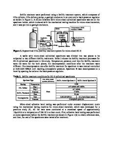
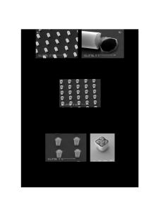
ABSTRACT Bond strength between three dimensional micro-sized cylindrical patterns and Si substrate has been evaluated to clarify the effects of the cylinder length vs. diameter ratio, i.e. the aspect ratio, on the bond strength. Cylindrical shape was employed for avoiding ambiguity of loading point under bend conditions. Multiple cylindrical specimens of an epoxy type photoresist, SU-8 with various lengths were fabricated on a silicon substrate under the same photolithographic condition. Bond strength between micro-sized SU-8 and Si substrate under bend loading mode was measured by a mechanical testing machine for micro-sized materials. The maximum bend moment is 9.6 x 10 -6 Nm in average and lineally increases with increasing the aspect ratio. On the other hand, the maximum load, i.e. maximum shear load is 106 mN in average and almost constant with increasing aspect ratio. This result suggests that the shear stress near the interface may cause the initiation of delamination. This phenomenon is discussed with three dimensional fracture observation and quantitative analysis of the line profile around the initiation site by AFM. INTRODUCTION Recently, chip-making technology has been significantly developed on the basis of twodimensional photolithography technique, which utilizes fine photoresist patterns on a substrate as masking for etching or molding for sputtering. It has become possible to fabricate more ultraprecise patterns with each passing year. This technique has widened to microfabrication for micro-electro-mechanical system (MEMS) devices in concert with three-dimensional microfabrication technique, micromachining, such as anisotropic etching, reactive ion etching (RIE), LIGA processing and so on. Micro-sized mechanical elements in MEMS devices are made up of the laminating fine pattern films using these techniques, thus, the devices include a large number of interfaces between dissimilar materials. There are many factors of stress concentration and defects at the interfaces, for example, natural defects, residual stress, difference of thermal expansion factor and/or that of Young’s moduli and so on. It brings about crack initiation in the vicinity of the interfaces during fabrication or in operation. Although the delamination is one of the most serious problems in MEMS devices, there are no standardized test methods to quantitatively evaluate bond strength for three dimensional microstructures. We have proposed quantitative measurement system for bond strength between three-dimensional micro-sized components and a substrate [1, 2]. A cylindrical shape has been employed as a micro-sized bond test specimen in this system, because multiple specimens can be easily fabrica
Data Loading...