Effects of Grain Boundary on the Ferroelectric Properties of Selectively Grown PZT Thin Films
- PDF / 1,722,446 Bytes
- 6 Pages / 417.6 x 639 pts Page_size
- 7 Downloads / 344 Views
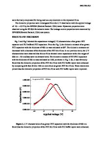
PZT thin films with and without grain boundary in the area measured. EXPERIMENT PZT(65/35) thin films were formed on Pt/SiO 2/Si substrates by RF magnetron sputtering at 3501C using multi-metal targets of Pb, Zr, and Ti. Base pressure before sputtering was below 1 x 10⁻⁵ Torr and the working pressure was 20mTorr during sputtering. PZT thin films (100nm) for seed layer were deposited on Pt/SiO 2/Si substrates and transformed into perovskite phase at 7001C by rapid thermal annealing (RTA). Seed islands (area : 13 tnnx 13 un, space : 40 gn) were patterned by conventional lithographic and etching method. PZT thin film (200nm) was deposited on the substrates having PZT seed islands. Fig. 1. shows the schematic diagram of the fabrication process of the single grained PZT array using PZT island seeds. Post annealing of the films was carried out in a furnace in an air ambient.
(a)
(b)
.-- PR mask
PPZT seed(lOOnm)
Si
(c)
e
SiO
(d)/
T
PZT island seed
PZT island seed
FIG. I. Schematic illustration of lateral crystallization of PZT thin films by PZT seeding. (a) seed layer deposition and crystallization at 700 0 by RTA method. (b) patterning by photo-lithography and wet etching of the seed layer. (c) top PZT thin film deposition on the PZT island seed. (d) plane view of the specimen. The growth behavior and the crystal structures of the films were investigated with an optical microscope and X-ray diffractometer, respectively. The conduction properties were measured using HP4140B pA meter and the polarization properties were examined by RT66A. Fatigue test was performed at room temperature with a square pulse of ± IOV at I kHz and I MHz. RESULTS AND DISCUSSION Fig. 2. shows optical micrographs with polarized light showing selective nucleation and growth of PZT thin films at different annealing temperatures. In Fig. 2(a), inner rounded rectangular patterns are perovskite PZT seeds with upper PZT films. It is clearly seen that rosettes were grown from the seeds. By cumulative annealing for 2 hours at 5801C and 2 hours at 600°C, 40 gnmx 40 un sized rectangular array of single-grained PZT thin films could be obtained as shown in Fig. 2(b). The PZT seed was 13 unx 13 gm and the laterally grown lengths were 14 un. In this method, location of the grain boundary could be controlled by controlling the sites for nucleation and growth.
316
PZT seed (a)
(b)
4
100/Ilm Grain boundary FIG. 2. Evolution of the lateral growth from the PZT seed. (a) after annealing at 5800 for 2 hours. (b) after addition of heat treatment at 600 °C for 2 hours to (a). Using thus obtained rectangular array of single-grained PZT thin films, we could measure the effects of the grain boundaries on the characteristics of the PZT thin films by locating the upper Pt electrode of 8 gmx 8 urn sized square right on the single grains, 1 grain boundary and 4 grain boundaries in a controlled manner shown in Fig. 3.
S•
Grain boundary PZT seed
Top electrode FIG. 3. Schematic illustration of the top electrode configurations for single grain, 1 grain bounda
Data Loading...