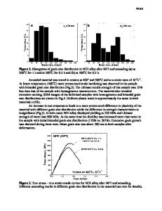
Effects of Location of Twin Boundaries and Grain Size on Plastic Deformation of Nanocrystalline Copper
- PDF / 938,026 Bytes
- 9 Pages / 593.972 x 792 pts Page_size
- 90 Downloads / 387 Views
TION
THE recent growth of research interest in nanocrystalline materials has manifested a significant attention to the mechanical behavior of materials with a typical average range of grain size finer than 100 nm. Great interest is originated from the unique properties of nanocrystalline materials, first observed and predicted by Gleiter’s pioneering work in materials[1] obtained by the gas condensation method and then verified by subsequent studies of the last decade. Substantial high strength and high hardness of nanocrystalline materials have made them attractive for many potential applications in microelectronic devices, magnetic storage media, and micro/nano electromechanical systems. In particular, due to enhanced wear resistance, nanocrystalline copper is considered to be a candidate for electrical contacts for dynamic systems. However, its lifetime is limited by the significantly deteriorated conductivity arisen from the electron scattering at the defects of metals such as high density of grain boundaries (GBs). Recent findings[2–6] revealed that both elevated conductivity and strength could be achieved simultaneously by introducing nanosized twin boundaries (TBs) in metals. Coherent TBs serve as the effective ARINA MARCHENKO, Graduate Student, and HAO ZHANG, Assistant Professor, are with the Department of Chemical and Materials Engineering, University of Alberta, Edmonton, AB T6G 2V4, Canada. Contact e-mail: [email protected] Manuscript submitted December 21, 2011. Article published online June 6, 2012 METALLURGICAL AND MATERIALS TRANSACTIONS A
blockage of dislocation motion and potent strengtheners, and possess extremely low electrical resistivity compared to GBs due to the smaller disordered structure. Therefore, a material containing TBs exhibits ultrahigh strength with the minimal loss in electrical conductivity. Over the last 10 years, a large number of experiments[7–14] and simulations[10,15–25] were performed to understand the strengthening mechanisms of nanotwins and to achieve the maximum strengthening effect through the control of the nanotwin microstructure in copper. To better understand the origin of ultrahigh strength in nanotwinned copper, Shen et al.[8] performed a computational analysis of tensile behavior of copper with a high density of nanoscale growth twins. The experimental investigations revealed that both the strength and the ductility increase with a decreasing twin lamella thickness due to the complex interaction between TBs and dislocations. Dao et al.[16] developed the concept of the TB-affected zone and evaluated possible optimization routes for strength and ductility. Recent experimental studies[9] showed the rate-controlling mechanism from the intratwin to TB-mediated process with decreasing twin lamellae thickness. According to Lu et al.,[9] the yield strength of the nanotwinned copper increases with decreasing twin spacing (k) to 15 nm, followed by a softening at smaller values. The softening mechanism is due to the increase in the density of preexisting dislocation sources at T
Data Loading...