Effects of Non-Planar Surfaces on the Growth of RF Magnetron Sputtered ZnO
- PDF / 1,547,060 Bytes
- 6 Pages / 612 x 792 pts (letter) Page_size
- 94 Downloads / 332 Views
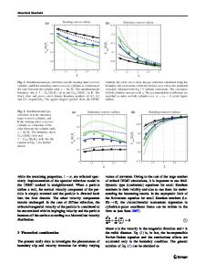
Effects of Non-Planar Surfaces on the Growth of RF Magnetron Sputtered ZnO A.S. Holland*, G.K. Reeves* and P.W. Leech** * School of Electrical & Computer Systems Engineering, RMIT University, Melbourne, Vic. 3001 Australia, ** Division of Manufacturing Science Technology, CSIRO, Clayton, Vic. 3169, Australia. ABSTRACT This paper describes the influence of the topography of a lithographically patterned substrate (aluminium electrodes on a CVD diamond film) on the uniformity of sputtered ZnO films. Diamond films with an average surface roughness of ~1nm, had aluminium electrodes (thickness 80nm, linewidth/space 2.6µm) patterned on them. ZnO was RF sputtered on to the substrate and the uniformity of the ZnO grain structure was examined using SEM, XRD and AFM. Abrupt changes in topography at the edges of the aluminium electrodes resulted in poor alignment of ZnO grains. SEM/AFM micrographs show misalignment of ZnO grains at the edges of the raised electrodes. When the electrodes were recessed into the diamond film, using a damascene-like process, the SEM/AFM micrographs showed improved grain uniformity of ZnO. XRD showed a significant increase in the c-axis (002) orientation and an absence of the (101) orientation. AFM micrographs also showed the improvement in the ZnO surface topography. These results may be of significance to high frequency Surface Acoustic Wave (SAW) devices. INTRODUCTION There have been a number of publications on the use of ZnO/Diamond layers on silicon substrates for SAW devices [1-5]. Diamond was investigated because it has the largest reported value of acoustic phase velocity [1] and hence CVD diamond thin films on silicon substrates are an attractive approach to making high frequency (GHz) SAW devices. However as diamond is not piezoelectric it needs to be coupled to a piezoelectric film in order to launch the acoustic wave. A ZnO film is commonly used because of its ease of deposition by sputtering [6] and its reasonably high phase velocity [1, 2, 7]. To achieve good piezoelectric activity, the ZnO films need to have an alignment as close as possible to the c-axis [8]. However, SEM micrographs show that misalignment of the c-axis of ZnO grains occurs at surface discontinuities due to surface roughness of either the diamond or the edge of the metal electrodes (interdigitated fingers) of the SAW transducer. Where a polished diamond film is used as the substrate, the raised metal electrode still presents a non-planar surface to the ZnO. To obtain the best possible alignment of the sputtered ZnO films, deposition on a completely planar substrate is highly desirable. Of the several SAW device substrate-electrode configurations possible [9], the most preferred types for giving high velocity and a good electromechanical coupling coefficient are what Nakahata et al [9] define as the type 1 and 2 devices. In these devices the metal electrode pattern is formed on the diamond surface followed by the deposition of ZnO. Thus the electrode is sandwiched at the ZnO-diamond interface. In such cases, in order
Data Loading...