Electric Degradation and Defect Formation of Silicon Due to Cu, Fe, and Ni Contamination
- PDF / 2,611,366 Bytes
- 12 Pages / 420.48 x 639 pts Page_size
- 26 Downloads / 278 Views
ELECTRIC DEGRADATION AND DEFECT FORMATION OF SILICON DUE TO Cu, Fe, AND Ni CONTAMINATION
SHUNTA NAITO AND TSUNEO NAKASHIZU* NSC Electron Corporation, Hikari, Yamaguchi, Japan *Nippon Steel Corporation, Hikari, Yamaguchi, Japan
Abstract Electric degradation of silicon wafer due to Cu, Fe, and Ni contamination has been studied using MCZ with low oxygen and CZ wafers. In the cases of Cu and Ni contamination, the electric properties depended on the characteristics of the starting wafers,, especially the type of conductance. The behavior of these metals in the low temperature region played an important role to understand the electric properties. On the contrary, no difference between p- and n-type wafers was observed in Fe contamination in our experiment. The surface defects were observed with high density in the MCZ wafers in Cu contamination. These defects were sensitive to the degradation of the MOS C-t generation lifetime. Making use of this relation, the efficiency of the extrinsic gettering was evaluated.
Introduction In the VLSI era, metal impurities such as transition metals are easily incorporated into the silicon wafer during device processing. In silicon, such unwanted impurities are Cu, Fe, and Ni. These impurities have high diffusivity at high temperature [11 and then form metal silicides or exist as a recombination or generation center of the minority carrier, which causes a serious electronic degradation. On account of making high quality device with high yield, these impurities should be taken away from device active region. Therefore some gettering treatments are inevitably applied to the starting wafer. The gettering treatment such as polysilicon back seal, sandblasting, ion implantation, laser irradiation, silicon nitride and intrinsic gettering have been extensively investigated by a large number of authors.[2-61 Among them the gettering efficiency has been estimated using intentionally contamination method. The impurity metals were monitored by haze pits, MOS generation, recombination lifetime, DLTS, and SPV. [7-131 These investigations strongly depend on the characteristics of the starting wafer. The oxygen concentration of the starting wafer is one of the most important factors which interacts with the impurity metals. As well as oxygen concentration, the doping impurities such as Phosphorus and Boron must be considered in the estimation of gettering efficiency. The purposes of this report are to investigate the relationship between impurity, such as dopant impurity or oxygen, and defect formation that are induced by metal contamination.
Mat. Res. Soc. Symp. Proc. Vol. 262. o1992 Materials Research Society
642
Experimental procedure
Wafer cleaning
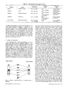
In order to clarify the correlation I between electrical degradation and the Intentional properties of crystal, such as oxygen and inati contamnaIon the dopant impurity, Czochralski (CZ) I wafers and magnetic Czochralski (MCZ) Oxidation wafers were used. Oxygen concentration 1 (JEIDA standard) ranges from 7.5 to 9.5 x 101 7 atoms/cm 3 in the CZ
Data Loading...