Electric Field Profile in Jic-Si:H P-I-N Devices
- PDF / 1,117,374 Bytes
- 6 Pages / 414.72 x 648 pts Page_size
- 13 Downloads / 302 Views
Mat. Res. Soc. Symp. Proc. Vol. 507 © 1998 Materials Research Society
Electric Field Determination To determine electric field profiles E(x) in p-i-n solar cells, two methods based on the TOF technique are available. The first one introduced by Street [8] relies on the current transient of a drifting sheet of charges. Beside the fact that this method has generally a poor spatial resolution (at least with standard TOF equipment), it is in most cases unsuitable for ptc-Si:H. The high capacitance observed in jWe-Si:H [5, 6] induces in fact a rather high RC-time constant which tends to distort the current transient.
----------------.f~iulight pulse
,•x )0
X
',"
0
0
L
x.
L
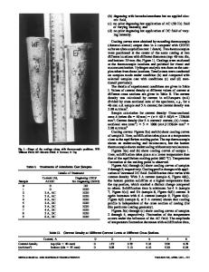
Figure 1: Determinationof the electric field profile E(x) according to Vanderhaghen et al. [9]: Cell under bias voltage Vbias (usually equal to 0 V) before probing of the internalfield (left) and during measurement (right). Zero field location is created at position xo where the photogenerated carriers, which have drifted from the front contact, accumulate. The second method, which avoids the drawback of the Street's technique, has been proposed by Vanderhaghen et al. [9]. It relies only on charge collection and does not require knowledge of the exact shape of the measured transients. This method consists of a modified TOF experiment, where an external electric field (pulsed, as in the standard TOF system) is superimposed on the internal field. The aim is to create a zero field location at position xo in the i layer (cf. Figure 1), where the internal field E(xo) is cancelled by the externally applied field Eext. By varying this external (forward) polarisation, one can change the position xo and, thus, probe the field profile E(x). The position xo (where the internal field E(xo) is equal to Eext) is
then given by the relation
Q=Q0 x°
-•
(1)
L Q the total photogenerated charge (which can be and sample thickness where L is the 0 determined by measuring the collection under high reverse polarisation). As a matter of fact, this method is "just" a reinterpretation of the charge collection curve, in terms of internal field distribution. As shown in previous papers of our group [10, 11], the performance of this technique can be decisively improved if one analyses the collection for both types of carriers (a semi-transparent contact must be provided for this purpose on both sides of the sample). A comprehensive discussion of this "bifacial" method may be found in Ref. [11]. As concerns the limits of this technique, two important points must be pointed out. First, the spatial resolution of the technique is limited by the charge generation gradient (i.e. by the penetration depth of the absorbed light). As a consequence, field values close to the p-i interface (or to the n-i interface) tend to be underestimated. All measurements presented in this paper were performed with an excitation light wavelength of 480 nm, giving an penetration depth of roughly 0.2 tim in Vc-Si:H and 0.02 gm in a-Si:H. Second, in order to obtain accumulation of charge (so a
Data Loading...


