Electrical and Optical Study of Charge Traps at Passivated GaAs Surfaces
- PDF / 2,657,961 Bytes
- 12 Pages / 417.6 x 639 pts Page_size
- 87 Downloads / 314 Views
Mat. Res. Soc. Symp. Proc. Vol. 573 ©1999 Materials Research Society
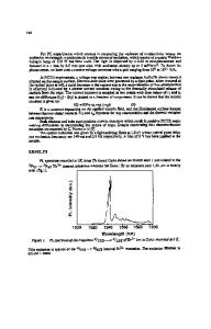
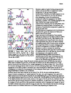
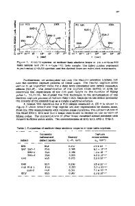
INTERFACE STATES CHARACTRIZED BY ELECTROREFLECTANCE Principl The surface region of GaAs-FET is passivated by dielectric films such as SiNx or Si0 2 and a large density of trapping states are present at the passivated interface. In order to discuss the effect of the charges induced by the interface states, energy distribution of the state density, Ns(E), has to be characterized. The task, however, has long been known to be difficult using the conventional electrical techniques based on capacitance measurements. The main source of the uncertainty in this type of techniques is the strong pinning of surface Fermi level due to those interface states since it is not appropriate in such a situation to analyze the state density from the comparison with ideal C-V curve. As an alternative approach, we have demonstrated that measurement of the so-called Franz-Keldysh oscillation (FKO) spectra in electroreflectance provides a way to assess the interface Fermi level, and thus Nj,(E), without relying on the external energy reference (i.e. ideal C-V curve)[4]. Energy distribution of interface-state density (Nss) can be obtained by measuring the semiconductor surface potential (V/,) as a function of applied voltage (VG). This is because, in a MIS capacitor, one can write CoX. (VG - V)
= (C,,+ CD).'.
(1)
which, then, reduces to Nss(V) = C,,(V)f/q
(2)
C1t Wg.)=. Co[( d f,)-1]dG - CS(V')
(3)
with
where C_, CD and C,, are the capacitance due to dielectric film, depletion layer and interface charges, respectively. The problem of obtaining Nj(E) thus reduces to an experimental determination of V, vs V.. In the conventional C-V technique, V/, has to be estimated from the measured capacitance values after comparing them with those for an ideal MIS capacitor. Here, surface majority-carrier accumulation and minority-carrier inversion are assumed to respectively yield C,. and Cm,,. This assumption is equivalent to setting energy references, Ec and Ev, for the determination of /,, which, however, is not necessarily justified for an interface with large NX(E). This is because the response (excursion) of y/, to applied voltage may be pinned alternatively at some position within the band gap due to a huge density of interface-state charges. Together with a possibility of interface traps partially responding at the measurement frequency of capacitance, a serious numerical uncertainty may arise depending on the combination of doping level and dielectric film thickness. On the contrary, Vtscan be evaluated by measuring the surface field using the ER technique without relying on the theoretical curve for y/. In modulated reflectance spectra of GaAs having finite surface band bending, an oscillatory features appear on the higher energy side of the fundamental gap transition, which are called Franz-Keldysh (FK) oscillations[5]. Since energy intervals of the oscillations is related to the magnitude of surface electric field, Fs, it is also connected with the surface band ben
Data Loading...