Electrical Characteristics and Device Applications of Zone-Melting-Recrystallized Si Films on SiO 2
- PDF / 3,790,453 Bytes
- 11 Pages / 417.6 x 639 pts Page_size
- 114 Downloads / 358 Views
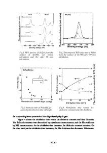
ELECTRICAL CHARACTERISTICS AND DEVICE APPLICATIONS OF ZONE-MELTING-RECRYSTALLIZED Si FILMS ON Si02 B-Y. Tsaur, John C. C. Fan, M. W. Geis, R. L. Chapman, S. R. J. Brueck, D. J. Silversmith, and R. W. Mountain Lincoln Laboratory, Massachusetts Institute of Technology, Lexington, Massachusetts 02173 ABSTRACT Device-quality Si films have been prepared by using graphite strip heaters for zone melting poly-Si films deposited on Si02-coated substrates. The electrical characteristics of these films have been studied by the fabrication and evaluation of thin-film resistors, MOSFETs and MOS capacitors. High yields of functional transistor arrays and ring oscillators with promising speed performance have been obtained for CMOS test circuit chips fabricated in recrystallized Si films on 2-inch-diameter Si wafers. Dualgate MOSFETs with a three-dimensional structure have been fabricated by using the zone-melting recrystallization technique. INTRODUCTION The utilization of dielectric isolation to achieve improved circuit performance for VLSI has stimulated great interest in the development of both Sion-insulator (SOI) materials and device isolation techniques. The materials and techniques that have been investigated include Si-on-sapphire (SOS), Si films prepared by graphoepitaxy [1], energy-beam-recrystallized Si films [2], Si films grown on Si0 2 by vapor-phase lateral overgrowth [3,4], isolation by oxygen implantation [5], and isolation by oxidation of porous Si [6]. We have recently developed [7,8] a recrystallization process that uses a movable graphite strip heater for zone melting poly-Si films, encapsulated with a composite Si02/Si 3 N4 layer, that have been deposited on Si02-coated Si substrates. Well oriented Si films up to 3 inches in diameter have been obtained by this technique [9]. The structural properties of zonemelting-recrystallized Si films have been reported elsewhere [8]. Briefly, unseeded films consist of elongated grains with (100) texture that are typically a few millimeters by a few centimeters on a side, with their long axis aligned approximately parallel to the direction of molten-zone motion. Within each grain there are many fine-line defects, typically spaced 20-30 vtmapart, that also run roughly parallel to the direction of molten-zone motion. TEM analysis indicates that these defects (which we call sub-boundaries) are dislocation arrays that are associated with angular deviations in orientation of the order of one degree or less. In this paper, the electrical characteristics of zone-melting recrystallized Si films will be described in detail. The majority-carrier transport properties and minority-carrier generation lifetime have been studied by the fabrication and evaluation of thin-film resistors, MOSFETs and MOS capacitors. Mobility enhancement occurs in Si films recrystallized on Si0 2 coated fused silica and sapphire substrates because of the large thermal stress in these films. Test CMOS circuit chips have been fabricated on 2inch-diameter SOI films to evaluate the material uniformity and spee
Data Loading...