Electrical Characterization of Defects Introduced in n-GaN During High Energy Proton and He-Ion Irradiation
- PDF / 402,238 Bytes
- 6 Pages / 420.48 x 639 pts Page_size
- 79 Downloads / 331 Views
he emission rate on electric field strength of defect ER3 is presented and discussed and we also present the true capture cross section of a deep lying defect, ER5. EXPERIMENTAL PROCEDURE For this study, 5 !tm thick GaN epitaxial layers grown at 1080 0 C on a 250 A GaN buffer layer on sapphire by metal-organic vapor phase epitaxy (MOVPE) were either exposed to 5.4 MeV He-ions from a 241Am radio-nuclide source or 2.0 MeV protons from a Van de Graaff accelerator. The nominally undoped GaN epitaxial layer had a free carrier concentration of approximately 2 - 3 x 1016 cm-3 . After boiling the samples in aqua-regia for ten minutes the samples were degreased [8]. Prior to ohmic contact fabrication the oxide layer was removed form the sample surface using a HCl: H20 (1 : 1) solution for 10 seconds [9]. The composite ohmic contact layer [10] was Ti/AVNi/Au (150 A/2200 A1400 k1500 A). The contact fabrication was followed by a five minute anneal at 500 TC in an inert gas atmosphere. Gold Schottky barrier diodes (SBDs), 0.5 mm in diameter and 3000 A thick were resistively deposited, these diodes had reverse leakage currents of the order of 10IO A at I V and ideality factors between 1.05 and 1.10. The samples were exposed to 5.4 MeV He-ions by placing them on an 24 'Am foil. The activity of the radionuclide being 192 itCi.cm 2 and the dose rate was 7.1 x 106 cm-2 .s-'. Sampes exposed to 2.0 MeV protons in the Van de Graaff accelerator recieved a dose of (3 + 1) x 1011 cm-2 at a dose rate of approximately 1 x 1010 cm-2s1. A twophase lock-in-amplifier-based (LIA) deep level transient spectroscopy (DLTS) system was used for the defect characterization in the as-grown material and the particle bombarded material. In order to simplify the determination of the emission kinetics of ER3 at different electrical field strengths in the space-charge region, isothermal DLTS was used. E, Fangetal [7]
-
10,
El and E2 , Gotzet al [12]
-
106 E5g 105
.6 3
E05
104 E2
U) 2
ER3 E2
103 E1
1
102 E2
El1
4 101 50
100
150
200 250 Temperature (K)
300
350
400
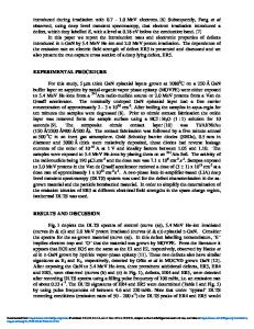
Figure 1: Curve (a): DLTS spectrum of as-grown MOVPE n-GaN. Curves (b) and (c): spectra recorded after 5.4 MeV He-ion irradiation. Curves (d) and (e): spectra recorded after 2.0 MeV proton irradiation. Curves (a) - (c) were recorded using a reverse bias (V,) of 2.0 V and filling pulse amplitudes (Vp)of 2.2 V. For curves (d) and (e). V. = 2.0 V and V_= 0.5 V.
2
4
R
8
ER1 1
n
1
IO00/T (K')
Figure 2: DLTS Arrhenius plots of defects in as grown n-GaN (open circles) and high ebergy Heion and proton irradiation (open squares). Other lines are for defects detected in GaN by other authors.
RESULTS AND DISCUSSION Fig. 1 depicts the DLTS spectra of control (curve (a)), 5.4 MeV He-ion irradiated (curves (b & c)) and 2.0 MeV proton irradiated (curves (d & e)) epitaxial n-GaN. Consider
the spectra for the as-grown material (curve (a)). In this defect labelling nomenclature, "E" implies electron trap and "0"that the material was grown by MOVPE. From the literature it appears that E
Data Loading...