Electrofluidic Assembly of Nanoelectromechanical Systems
- PDF / 211,462 Bytes
- 6 Pages / 612 x 792 pts (letter) Page_size
- 24 Downloads / 326 Views
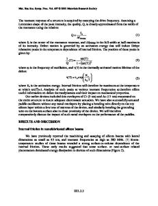
Electrofluidic Assembly of Nanoelectromechanical Systems Stephane Evoy1, Ben Hailer, and Martin Duemling Department of Electrical and Computer Engineering, Virginia Tech, Blacksburg, VA 24061 Benjamin R. Martin, Thomas E. Mallouk, Irena Kratochvilova and Theresa S. Mayer Department of Chemistry and Department of Electrical Engineering, Penn State University, University Park, PA 16802 ABSTRACT Recent advances in surface nanomachining have allowed the fabrication of mechanical structures with dimensions reaching 20 nm, and resonant frequencies in the 100s of MHz. Structural issues prevent the ``top-down'' surface machining of high-quality NEMS resonators. Such systems are alternatively to be bestowed by ``bottom-up'' manufacturing technologies. We report the surface assembly of RF-range NEMS. Using electrofluidic assembly, we have successfully positioned Rh mechanical beams onto specific sites of a silicon circuit. With diameters as small as 250 nm and lengths varying from 2 to 3 µm, preliminary results show mechanical resonances ranging from 5 MHz to 80 MHz, and quality factors reaching 500. We also report the development of nanostructured NEMS for sensor applications, and present strategies for their deployment in integrative nanosystems. INTRODUCTION Nanometer scale science and engineering revolutionizes materials manufacturing, and the range of functionalities that can be accessed. Microelectromechanical systems (MEMS) have already transformed the microelectronics industry by providing a new range of integrative functionalities to several applications. Recent advances in surface nanomachining have allowed the fabrication of mechanical structures with dimensions reaching 20 nm (Fig 1) [1]. The fabrication of such nanoelectromechanical systems (NEMS) usually involves the lateral patterning of a single crystal mechanical layer and release through etching of an underlying sacrificial material [2,3]. These devices are of interest for the development of highly sensitive sensors, and the integration of low power RF-range nanomechanical signal processors.
a)
b)
c)
250 nm
d)
200 nm
Fig. 1: NEMS. a) 2 µm x 3 µm Si paddle supported by 150 nm-wide beams (from Evoy, Carr, et al. [4-8]) b) 50 nmwide 100 MHz-range Si resonant beams (from Carr, Evoy, et al. [9]). High aspect ratio laterally-resonant 100 MHzrange Si NEMS (Barnhart et al [10]) c) Assembled 80 MHz Rh NEMS.
1
Now at the University of Pennsylvania: [email protected]
B4.4.1
Specifically, Carr, Evoy et al. have reported Si prototype NEMS with frequencies reaching 380 MHz [4-9]. However, we have also reported that surface phenomena degrade the performance of these devices [5-7], preventing the "top-down'' machining of high-quality NEMS. Such devices are alternatively to be bestowed by "bottom-up'' approaches (Fig 1d). We report the surface assembly of RF-range NEMS. Using an electrofluidic technique developed by Smith et al. [11], we have positioned Rh mechanical beams onto specific sites of a silicon circuit. Platinum group metals have been dubbed noble meta
Data Loading...