Electronic Properties of Dislocations in Heavily Dislocated Quantum well Structures: Doping Effects
- PDF / 801,414 Bytes
- 6 Pages / 420.48 x 639 pts Page_size
- 76 Downloads / 311 Views
ELECTRONIC PROPERTIES OF DISLOCATIONS IN HEAVILY DISLOCATED QUANTUM WELL STRUCTURES: DOPING EFFECTS
T. Y. LIU, P. M. PETROFF, H. KROEMER, AND A. C. GOSSARD Department of Electrical and Computer Engineering, and Materials Department, University of California at Santa Barbara, Santa Barbara, CA 93106
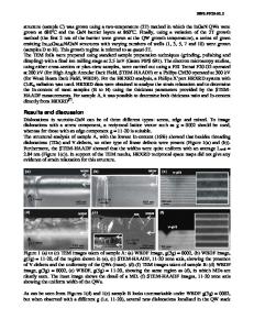
ABSTRACT 2 In heavily dislocated GaAs (dislocation density of 108cm- ), the low-temperature cathodoluminescence efficiency of quantum wells and superlattices is dramatically higher than that of a bulk-like layer. Furthermore, the luminescence efficiency can be further improved by doping the barriers of the GaAs/(AI,Ga)As multi-quantum well structures with beryllium (Be). Two quite different possible models for this observation are discussed: One assumes that the effect is due to the expulsion of dislocation kinks from the wells, the other that it is due to the effect of well width fluctuations.
INTRODUCTION The electronic quality of epitaxially grown lattice-mismatched semiconductors, such as GaAs-onSi, is limited by the presence of misfit dislocations. The misfit dislocations are usually not confined to the misfit plane, but some of them always propagate into the epitaxial layer, forming a network of threading dislocations which have been related to a variety of non-radiative 2 recombination activities [1]. Dislocation densities of the order of 108 cm- are typical, and these values do not depend strongly on the amount of lattice mismatch [2]. 2 The quality of a bulk-like thick epitaxial layer with 108 cm- of dislocations is such that it is essentially useless for opto-electronic minority carrier devices such as lasers. However, quantum wel/(QW) structures grown on lattice-mismatched substrates seem to have a much higher luminescence efficiency (defined as the ratio of the peak luminescence intensity of a heavily dislocated QW or bulk layer to that of an identical structure without dislocations, or with a dislocation density similar to that of commercially available GaAs substrates, which is about 104 cm-2 only). This is exemplified by the observation that - at least so far - all reports of successful cw room-temperature lasers employing GaAs/(AI,Ga)As grown on silicon substrates involve quantum well lasers rather than "ordinary" double-heterostructure lasers [3]. To understand better the effects of QWs on modifying the electronic properties of dislocations, we have performed a series of experiments to look at the material quality in heavily dislocated materials, using low-temperature cathodoluminescence (CL) as a highly sensitive probe. In our initial work on this subject [4,5], performed on Si substrates, we had shown that, when the dislocated material is present in the form of multi-quantum-well (MQW) or superlattice (SL) structures rather than bulk-like material, its luminescence efficiency remains much higher than that of a bulk-like equally dislocated layer. As an explanation, we proposed a model, according to which kinks along the dislocation lines act as the non-radiative recombination centers responsible for
Data Loading...