Electronic Structure of Epitaxial SiO 2 /Si(100) Interfaces
- PDF / 1,163,785 Bytes
- 6 Pages / 420.48 x 639 pts Page_size
- 66 Downloads / 380 Views
ELECTRONIC STRUCTURE OF EPITAXIAL SiO 2 /Si(100)
INTERFACES
T. Motooka Institute of Applied Physics,
University of Tsukuba,
Ibaraki 305
ABSTRACT The local densities of states (LDOS) of epitaxial SiO, layers on Si(100) surfaces have been calculated using the recursion method combined with the Harrison's universal tightbinding model. The interface states associated with strained epitaxial layers of 0-cristobalite (f2X[2)R45° and tridymite (1010)11 Si(100) were examined. In the 0-cristobalite layer, gap states due to the surface Si dangling bonds apoeared while they were eliminated by H termination. In the tridymite layer, the interface states primarily composed of the surface Si back bonds appeared near the Si conduction band minimum. Comparing the calculated DOS with photoelectron spectra for initial oxidation processes of clean Si(100), it was found that the valence band spectrum from the initial oxide formed at -300r resembled that of the P -cristobalite layer.
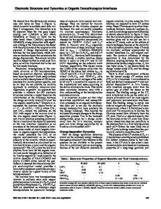
INTRODUCTION The Si0 2 /Si interface has been extensively investigated for its importance in Si MOS technology. [1] Various kinds of measurements such as photoelectron spectroscopy and transmission electron microscopy (TEM) have been utilized to characterize the atomic and electronic structure at the Si0 2 /Si interface. It is generally known that there exists a thin suboxide region, SiOx (x Si(100). The interface states appeared near the Si conduction band minimum and were primarily composed of the surface Si back bonds. a, The calculated DOS from 5-layer epitaxialPFig.1 Crystalline Si0 2 structures: cristobalite and tridymite t (a) P crystaline and struc were compared with measured e. ( -cristobalite and (b)tridymit valence spectra for initial oxidation of Si(100) substrates in a UHV chamber. [51 The results suggest that the initial oxidation layer is likely to form a $cristobalite structure at -300 *C.
CRYSTALLINE Si0 SURFACES
2
AND STRAINED-LAYER-EPITAXIAL
Si0 2 ON Si(1O0)
Figure I shows bulk 0-cristobalite and tridymite[6] which possibly form epitaxial layers on Si(l00) surfaces as described below. Both of these crystalline structures are constructed by similar units as shown in Figure 1. The Si-O-Si angle is 180' in both cases, but the oxygen configuration around the Si-O-Si axis is staggered in 0-cristobalite while it is eclipsed in tridymite. This results in a diamond (hexagonal) structure for 0-cristobalite while (tridymite). Bulk V-cristobalite is formed at =30O0
tridynite at =200r .[6] Strained-epitaxial layers of 0-cristobalite and tridymite on Si(l00) are illustrated in Figure 2. The unit length of the f.c.c. in P-cristobalite is 7.16A, approximately T2 times longer than
205
that of the Si f.c.c.
lattice,
5.43A. Thus, strained-layer epitaxy is possible by rotating
0
(a)
Si
S 0
the axis of $-cristobalite by 45' which is known as a ([2xT2)R45* structure. [7] The lattice mismatch associated with
this epitaxial interface is =7% and half of the surface Si atoms connect to the 0 atoms while the other half are free. Tridymite ha
Data Loading...