Electronic transport and microstructure in MoSi 2 thin films
- PDF / 975,786 Bytes
- 10 Pages / 594 x 810 pts Page_size
- 58 Downloads / 382 Views
J. Mater. Res. 1 (3), May/Jun 1986 http://journals.cambridge.org
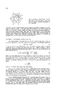
near the Fermi energy were said to be due to a mixing of silicon 3s and 2>p states with molybdenum 4s1 and 5d states. The partial filling of some bands leads to metallic conduction. It was suggested then that the electron efTo our knowledge, the only detailed calculation of the electronic energy band structure was published last year.21 The theoretical density of states is shown in Fig. 1 (a). The relevant features of the figure for this work are the existence of a low density of states at the Fermi energy, which suggests a low effective carrier density, and the possibility of a negative effective mass, which would give rise to hole conduction. A 1957 investigation concluded that MoSi2 and a number of other transition metal silicides are "essentially metallic,"22 based on resistivity and magnetic susceptibility measurements. An analysis of bond lengths showed that metal-metal and silicon-silicon bond lengths are so large that the observed behavior must be associated with the character of the strong metal-silicon bonds. A recent photoemission study of the compound indicated that the primary character of the states near EF is metal d derived, but that silicon s- and^-derived states are present at the Fermi energy as well.23 Here EF was found to be near a minimum in the density of states, which is represented in Fig. 1 (b) by an experimentally obtained photoemission spectrum that quite resembles the theoretical state distribution in Fig. l ( a ) . Peaks in the photoemission spectrum were identified by Weaver et al. with the assistance of band structure calculations for other Mo-Si compounds. Finally, recent measurements of the dielectric function of MoSi2 indicated a major peak in the density of states at about 2.5 eV below EF, in agreement with both parts of Fig. I. 24 A "bulk" MoSi2 resistivity value of 21.5/ufl cm was
0003-6951 /86/030493-10$01.75
Downloaded: 18 Mar 2015
© 1986 Materials Research Society
493
IP address: 140.182.176.13
T. L Martin and J. E. Mahan: Transport and microstructure in MoSi2 thin films
TABLE I. Previously reported resistivity values for tetragonal MoSi2 thin films.
Resistivity
Deposition method
40/ifl cm 50
coevaporation cosputtering
58
sputtering of alternating Mo and Si layers on polysilicon metal evaporation onto 750 °C silicon substrate cosputtering or coevaporation sputtering of MoSi2 silane silicidation of sputtered Mo cosputtering
65
70 80 80
84
100
coevaporation
100
cosputtering
105
cosputtering
100-150
cosputtering
130
sputtering
reported in 1951,25 which is close to the room temperature intrinsic resistivity we have obtained. A 1964 transport properties investigation was based on samples formed from sintered powders. Hall measurements indicated predominantly "p-type" conduction and that MoSi2 is a "high" mobility metallic conductor.26 It was stated that the low concentration and positive sign of the charge carriers were due to the fact that the conductivity is mainly via "a broad band belo
Data Loading...


