Electronic Transport Properties of ZnSe Layers on GaAs
- PDF / 455,630 Bytes
- 6 Pages / 420.48 x 639 pts Page_size
- 71 Downloads / 426 Views
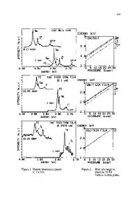
Electronic Transport Properties of ZnSe Layers on GaAs T. MARSHALL, S. COLAK, H. VAN HOUTEN, J. PETRUZZELLO, B. GREENBERG, and D. CAMMACK Philips Laboratories, North American Philips Corporation, Briarcliff Manor, NY 10510 ABSTRACT The electronic transport properties of ZnSe layers grown by MBE on GaAs substrates are studied by small-signal ac admittance, dc current-voltage, and Hall effect measurements. This work is supplemented by a study of TEM and x-ray rocking curve data. We find that the transport characteristics are strongly affected by the properties of the ZnSe/GaAs interface. From the dc and ac measurements, we determine the total barrier height at the interface of thick (1-6 pm) ZnSe layers on n+-GaAs, and find that it is in general voltage dependent. While some samples are found to have a very high peak mobility (> 10,000cm 2 /Vsec), an anomalous reduction in the mobility in a large fraction of the samples is found, and attributed to the presence of nonuniform space charge regions. INTRODUCTION There has been much recent progress in improving the quality of ZnSe epilayers grown on GaAs (100) substrates, in part because of the use of higher-purity source materials [1-51. Impurity concentrations as low as 101" cm- 3 have been achieved [2,51, and narrow donor-bound-exciton PL linewidths have been observed [6,7]. We present results on the electrical characterization of ZnSe epilayers grown with two different purity grades of Zn and Se source material. Vertical ac and dc measurements and lateral transport were studied. Vertical current vs. voltage (I-V) and capacitance vs. voltage (C-V) measurements allow a direct determination of the heterojunction (HJ) barrier height $Joj as well as of the carrier concentration. Additionally, analysis of spreading effects in the admittance data vs. frequency permits the extraction of the epilayer resistivity. Lateral Hall-effect measurements provide more quantitative and complementary information about "bulk" properties of the epilayers. Some samples had unprecedentedly high peak mobility, in excess of 10,000 cm 2 /Vsec at about 50 K. However, we found puzzling behavior in many similarly prepared samples, which showed both peak and room temperature (RT) mobility well below that of the best samples. The results are discussed together with additional information from TEM and x-ray structural data. MBE GROWTH AND SAMPLE FABRICATION The ZnSe epilayers were grown in a Varian Gen II MBE system on GaAs (100) substrates. The substrates received a standard chemical etch [8] prior to indium mounting, and were heated in vacuum to desorb the oxide layer before starting growth. Epilayers for this study were grown using elemental Zn and Se sources. Initial work was done using Zn and Se of 6N purity; subsequent growths were done with Osaka Asahi super-grade materials. All epilayers grown were above the critical layer thickness for pseudomorphic growth, and thus the hetero-interface has a linear density of misfit dislocations of about 10/jim [9]. Most samples studied had a Zn/Se beam pres
Data Loading...