Enhanced Blue Sensitivity in ITO/a-SiN x :H/a-Si:H MIS Photodetectors
- PDF / 563,409 Bytes
- 6 Pages / 612 x 792 pts (letter) Page_size
- 63 Downloads / 309 Views
A21.6.1
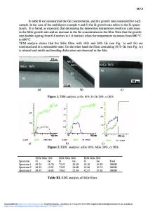
Enhanced Blue Sensitivity in ITO/a-SiNx:H/a-Si:H MIS Photodetectors S. Tao, Y. Vygranenko, and A. Nathan Electrical and Computer Engineering, University of Waterloo, Waterloo, Ontario N2L 3G1, Canada ABSTRACT We report an ITO/a-SiNx:H/a-Si:H MIS photodetector with improved performance in terms of its dark current, stability, and spectral response in the blue region. The a-Si:H and a-SiNx:H thin film layers were deposited by plasma-enhanced chemical vapor deposition (PECVD) on a glass substrate with patterned Mo back contact. The ITO was polycrystalline with a wide band gap (> 3.75 eV) and was deposited at room temperature by magnetron sputtering. SIMS (Secondary Ion Mass Spectrometer) measurements show that an ultra thin a-SiNx:H film (a few nm) can effectively block the diffusion of oxygen from the ITO to the a-Si:H. In addition, the insulator layer provides a barrier for electrons, which serves to reduce the dark current. This is in contrast to the ITO/a-Si:H Schottky photodiode whose electrical and optical performance is impaired by the large defect density at the interface due to impurity diffusion from the ITO layer. At a reverse bias of 1 V, the dark current density of the MIS photodetector is as low as 4 nA/cm2. Photoresponse measurements show a dramatically enhanced sensitivity in the UV/blue spectral region. A high quantum efficiency (~80%) is achieved at a wavelength of 440 nm, which can be attributed to reduction of both optical and recombination loses by virtue of the highly transparent polycrystalline ITO and the low defect density at the a-SiNx:H/a-Si:H interface. INTRODUCTION Hydrogenated amorphous silicon (a-Si:H) technology is widely used in large area imaging applications [1]. Here, the sensing element is either the p-i-n or Schottky photodiode [2]. The latter, with an ITO front contact, has advantages in terms of fabrication simplicity, high photosensitivity and fast response [3]. However, the diffusion of impurities (O, In, Sn) from the ITO to the a-Si:H undermines the integrity of the Schottky interface, which leads to high dark current [4][5]. It has been recently proposed that use of a thin insulator layer (e.g. a-SiNx:H) between the ITO and the a-Si:H can suppress the electron injection from the ITO through the Schottky interface [6]. In this paper, an ITO/a-SiNx:H/a-Si:H MIS photodetector is presented, which exhibits a low dark current, good stability, and enhanced short-wavelength photoresponse. EXPERIMENTS A cross-sectional diagram of the ITO/a-SiNx:H/a-Si:H MIS photodetector is illustrated in Figure 1. The n+a-Si:H, intrinsic a-Si:H, and thin a-SiNx:H films were deposited consecutively on a Mo coated 7059 corning glass substrate, followed by the sputter deposition of a 2000 Åpolycrystalline ITO film at room temperature to form the MIS structure. The ITO layer was patterned to define and isolate the MIS structure using reactive ion etching (RIE). All samples had the same thickness of n+ and intrinsic a-Si:H layers, and were 1000 Å and 7500 Å, respectively. Different thicknesses of
Data Loading...