Evaluation of Contact and Via Step Coverage Using a Novel Two-Step Titanium Nitride Barrier Deposition Process
- PDF / 740,178 Bytes
- 6 Pages / 612 x 792 pts (letter) Page_size
- 62 Downloads / 355 Views
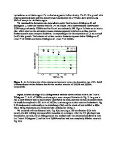
Evaluation of Contact and Via Step Coverage Using a Novel Two-Step Titanium Nitride Barrier Deposition Process Ardy Sidhwa, Chuck Spinner, Todd Gandy STMicroelectronics, Inc.; 1000 East Bell Road; Phoenix AZ 85255 and William Brown, Simon Ang, Hameed Naseem, and Richard Ulrich University of Arkansas; Department of Electrical Engineering 3217 Bell Engineering Center; Fayetteville AR 72701 Abstract Aluminum plug technologies are still used for many different semiconductor device applications and are cost-effective processes. However, there are some disadvantages associated with them. The key disadvantage is aluminum junction spiking caused by aluminum diffusing down into the silicon substrate and silicon diffusing up into the aluminum plug due to a poor titanium nitride (TiN) barrier [1]. The tungsten plug process is primarily used for 0.5µm and smaller technologies. Titanium nitride barrier material plays an important role as an underlayer for tungsten plugs to prevent tungsten hexafluoride (WF6 ) from attacking the titanium (Ti) film [2]. The role of the TiN barrier is to retard or prevent diffusion of the materials that the TiN layer separates [3]. In this work, the authors investigated the TiN barrier film properties with respect to nitrogen flows at two different power set points and argon gas flows. Different experiments were performed to understand the properties of the TiN film with respect to process variables. Single-step and dual-step TiN barrier processes were studied for contact and via step coverage profiles used for aluminum and tungsten plug technologies. Introduction Device aspect ratios and dimensions at the contact and via levels for old and new technologies are driving PVD-based metallization to its full limit. Contact and via structures, while not posing the same rigorous dimensional problems as high aspect ratios, still suffer from problems associated with PVD sputtering of titanium (Ti) and titanium nitride (TiN) films [4]. These problems include poor barrier quality, which can lead to wormholes and volcanoes for tungsten plug technologies. Non-conformal step coverage leads to aluminum junction spiking for aluminum (Al) plugs due to poor TiN barrier quality. Figure 1a shows a TEM micrograph of aluminum junction spiking due to poor quality TiN barrier step coverage. Figure 1b shows volcanoes for a tungsten plug process due to poor barrier quality. Many types of metallization schemes are being investigated for via structures for 0.9µm to 0.18µm technologies. One common strategy is simply to extend the existing PVD-based solution to all technologies. This solution involves deposition of a Ti film to getter existing aluminum oxide and reduces via resistance, followed by a TiN film to act as a barrier and adhesion level for the Al or W plug metallization.
Volcano
AlCu spiking through
TiN spiking through AlCu TiN
Figure 1a
B12.10.1
Figure 1b
Purpose for the Development of New Titanium Nitride (TiN) Barrier Process Titanium nitride (TiN) thin films are the most commonly Volcano used films for b
Data Loading...