Evaluation of Electric Potential at Metal-insulator Interface Using Electron Spectroscopy and Kelvin Probe Techniques
- PDF / 218,745 Bytes
- 9 Pages / 612 x 792 pts (letter) Page_size
- 65 Downloads / 422 Views
0894-LL02-02.1
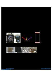
Evaluation of Electric Potential at Metal-insulator Interface Using Electron Spectroscopy and Kelvin Probe Techniques Michiko Yoshitake Nanomaterials Laboratory, National Institute for Materials Science Tsukuba, 305-0003, Japan ABSTRACT The potential of applying photoelectron spectroscopic and Kelvin probe methods for the interface potential evaluation of materials prepared by combinatorial processes is demonstrated. The physical basis for the evaluation of the interface potential by photoelectron spectroscopy is given. Then, the imaging capability of photoelectron spectroscopy is demonstrated using a two-dimensionally patterned specimen. Finally, the examples of interface potential evaluation with photoelectron spectroscopy and Kelvin probe are presented. Through the evaluation of interface potential with this method, it is possible to deduce the energy level diagram across the interface between two materials with different electron properties. INTRODUCTION In combinatorial material processing, materials prepared under different conditions – compositions, thickness, and so forth - are often located in two-dimensional coordinates. Hence, combinatorial methods for material characterization are mostly based on imaging techniques. In other words, any existing imaging technique has potential to be applied as a combinatorial characterization method. The characterization of an interface by electron spectroscopic methods is a topic of this paper. These methods can be extended to an imaging mode. Electron spectroscopic techniques have been utilized to observe chemical compositions and chemical binding states. The paper will show that they also can work as good tools to evaluate electric properties at interfaces through the correlative analysis of binding energy shifts. In the field of electronic devices, the role of interface has become more and more important. The position of the conduction band minimum and valence band maximum in both materials in contact are key factors to determine contact potential, excitation photon energy of photo devices and so forth. Due to downsizing of devices, electron spectroscopic techniques, whose detection depth is rather shallow, have increasingly proved to be a powerful tool to evaluate interfaces in materials research for electron devices. Here, how X-ray and UV photoelectron spectroscopy (XPS and UPS) combined with Kelvin probe method give useful information about the electric property at metal-insulator and semiconductor-insulator interfaces, is demonstrated. Since photoelectron spectroscopic techniques have imaging capability in the order of micrometer range, it will be applied to the combinatorial characterization. The principle of the evaluation and the way of analyzing XPS or UPS spectra for the above purpose will be discussed. A couple of examples of electric potential analysis at interfaces will be given. METHODS The schematic energy diagrams of a conductive material A and a material B with a band gap (CB-VB) with and without contact are shown in figure 1. When bot
Data Loading...