Extended State Mobility and Tail State Distribution of a-Si 1-x Ge x :H Alloys
- PDF / 358,766 Bytes
- 6 Pages / 420.48 x 639 pts Page_size
- 101 Downloads / 329 Views
EXTENDED STATE NOBILITY AND TAIL STATE DISTRIBUTION OF a-Si 1 _xGex:H ALLOYS C. E. Nebel,
H. C. Weller, G. H. Bauer
Institut f. Physikalische Elektronik, Universitaet Stuttgart, Pfaffenwaldring 47, D-7000 Stuttgart 80, F. R. Germany
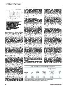
ABSTRACT Time-of-flight (TOF) and charge collection measurements are evaluated to determine electron transport quality of a-Si 1 Ge :H for 0 < x 5 0.3. The drift mobility data are used to calculate the -aiT state distribution at the conduction band, which turns out to be of hybrid structure (flat linear followed by a steep exponential decay). By incorporation of Ge additional localization introduced by chemical disorder broadens the band tail. The dangling bond density, calculated from electron ADTe products, also dramatically increases. Both effects contribute to the drop of photoelectronic quality of a-Si 1 xGe :H alloys. In addition it is shown tRat the extended state mobility deduced from TOF experiments reflects a tunneling transport mechanism in localized states above a dominant transport level that separates states with high tunnel probability from states where carriers propagate via thermal release from and capture into localized states. INTRODUCTION Alloying of amorphous Si films by Ge is of considerable interest regarding thin film photovoltaics with band gaps optimized with respect to solar radiation distribution as well as for multispectral solar cells. However the photoconductive properties of alloys so far prepared are inferior to a-Si:H. In this paper we discuss results from TOF and charge collection measurements intending to improve our understanding of the nature of states that control transport and recombination of electrons that govern the quality of a-SiGe:H alloys [1]. EXPERIMENTAL The principle measurements used to study trapping in tail states and recombination via dangling bonds (db) are time-of-flight (TOF) photoconductivity, and charge collection. In order to determine the variation of optoelectronic quality versus Ge incorporation, samples have been prepared in a glow discharge of SiH 4 and SiH4 /GeH 4 mixtures in a diode reactor only varying the SiH 4/GeH 4 ratio [2]. The increase of Ge concentration (x = 0, 0.025, 0.11, 0.2, 0.3) derived from XPS data corresponds to a decrease of optical gap (E = 1 75eV, 1.74eV, 1.69eV, 1.62eV, 1.55eV). A convehtional TOF setup and sandwich contact configuration (substrate/ Cr/a-Si 1 _xGex:H/semitransparent Cr) are used to measure either the drift mobjlity AD at different temperatures (120K - 400K) and electric fields (10OV/cm - 10'V/cm) or the mobility-lifetime product IDTe depending on the charge collection Q, which is the time integral of te current pulse. The indication that carriers have completely crossed the sample is when Q is observed to be independent of the applied electric field F, and the defined transit time then gives the drift mobility. Mobility a of electrons for 0 • x < 0.2 is shown in Fig. 1 in a and Ge conlog(p 0 D) versus 19T plot for different electric field strengths tent. Transit time of carriers w
Data Loading...