Extreme Supersaturation of Oxygen in Low Temperature Epitaxial Silicon and Silicon-Germanium Alloys
- PDF / 270,158 Bytes
- 6 Pages / 420.48 x 639 pts Page_size
- 91 Downloads / 353 Views
EXTREME SUPERSATURATION OF OXYGEN IN LOW TEMPERATURE EPITAXIAL SILICON AND SILICON-GERMANIUM ALLOYS P.V. SCHWARTZ*, J.C. STURM*, P.M. GARONE*, AND S.A. SCHWARZ** *Department of Electrical Engineering, Princeton University, Princeton, New Jersey 08544 **Bell Communications Research, Inc., Red Bank, New Jersey 07701
AbsqtrartWe report the low temperature growth (625 - 700 *C) of epitaxial silicon and silicon-germanium alloy films by vapor phase techniques with oxygen concentrations approximately 1020 cm- 3 . These concentrations are well above the accepted solid solubility for oxygen in silicon. The films, however, have excellent structural and electrical properties with virtually no stacking faults or "haze". Infrared transmission analysis suggests the possible presence of OH, but the exact nature of the oxygen is not known. Introduction Generally, oxygen is a harmful contaminant in epitaxial films. The presence of oxygen precipitates may give rise to stacking faults in the epitaxial film and in extreme cases cause haze on the surface of the wafer. Here we report the low temperature growth of crystalline epitaxial films with oxygen 3 concentrations reaching 1020 cm- . Growth The samples were grown by Limited Reaction Processing (LRP) [1], a combination of Chemical Vapor Deposition (CVD) and Rapid Thermal Processing (RTP). The reactor is a lamp heated system which utilizes no susceptor. Each sample is suspended on quartz pins in a quartz wall chamber above a bank of twelve tungsten halogen lamps. The radiation from the lamps heats the wafer directly while leaving the chamber wall cool. Another feature of the system is that it has no load lock. During each loading process, the chamber must be vented to atmosphere. This is a possible source of contamination to the system. The epitaxial films are grown at a pressure of 6 torr. Dichlorosilane and germane are used as the source gases and hydrogen is used as the carrier gas. Before growth, each sample undergoes a high temperature clean (1200 0C). The clean is done in a hydrogen atmosphere and removes impurities from the wafer surface. The growth process begins with the growth of a silicon buffer layer (1000 OC), followed by a temperature drop to 0 700 C for growth of Si epitaxial layers or to 625 0C for growth of Si i-xGex epitaxial layers.
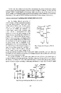
Typical sample structures are
shown in Figure 1. The epitaxial films grown at low temperature have excellent structural characteristics. They are all single crystals and
Mat. Res. Soc. Symp. Proc. Vol. 163. ©1990 Materials Research Society
592
exhibit no observable haze on the surface of the wafer in either the visible or the ultra-violet regions. In plan view TEM, we notice misfit dislocations in some Si i-xGe x strained layer samples, but stacking faults are seldom observed. Stacking virtually absent from our silicon samples as well.
faults are
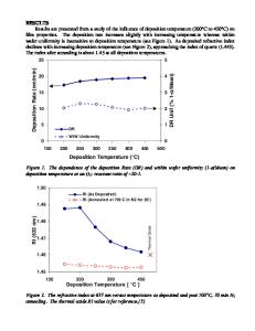
Characterization In order to characterize our system, we performed Secondary Ion Mass Spectroscopy (SIMS), calibrated against implant standards, on our epitaxial samples. In Figure 2,
Data Loading...