Fabrication and Characterization of Copper Oxide Resistive Memory Devices
- PDF / 302,705 Bytes
- 6 Pages / 432 x 648 pts Page_size
- 2 Downloads / 416 Views
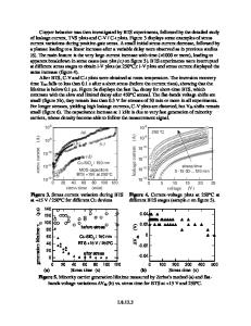
Fabrication and Characterization of Copper Oxide Resistive Memory Devices S.M. Bishop1, B.D. Briggs1, Z.P. Rice1, S. Addepalli1, N.R. McDonald2, and N.C. Cady1 1 University at Albany, SUNY, College of Nanoscale Science and Engineering, Albany, NY 12203, U.S.A 2 Air Force Research Laboratory/RITC, Rome, NY 13441, USA ABSTRACT Three synthesis techniques have been explored as routes to produce copper oxide for use in resistive memory devices (RMDs). The major results and their impact on device currentvoltage characteristics are summarized. The majority of the devices fabricated from thermally oxidized copper exhibited a diode-like behavior independent of the top electrode. When these devices were etched to form mesa structures, bipolar switching was observed with set voltages 10 years have also been predicted [2,3]. Despite this progress, there is a significant lack of information available in the open literature on the fabrication of these devices. In this work, a systematic investigation has been performed to determine how the oxide synthesis technique, film properties, and the device fabrication process impact the switching behavior of RMDs. The technical challenges encountered with each synthesis technique will be discussed, and the process conditions employed to produce switchable oxide thin films will be introduced. EXPERIMENTAL PROCEDURE Copper oxide was synthesized by oxidation and reactive sputtering on top of 1 μm thick copper thin films that were electroplated on Ta/TaN/SiOx/SixNy/Si. Thermal oxidation of the copper electrode was performed at 200-400°C in air at atmospheric pressure. Plasma oxidation was performed at RT and 280°C with an oxygen flow rate of 1-14 slm, a pressure range of 0.52.5 Torr, and an RF power range of 300-1000 Watts. Copper oxide was deposited by room temperature reactive sputtering at 1x10⁻² Torr and 2000 W; the oxygen flow rate was maintained at 20 sccm, while the argon flow rate ranged from 3.5-20 sccm. Scanning electron microscopy (SEM), atomic force microscopy (AFM), and transmission electron microscopy (TEM) were employed to analyze the microstructure of the resulting films. X-ray diffraction (XRD) was
55
utilized to determine the phase(s) of copper oxide present. Devices were fabricated by patterning top electrodes using either a shadow mask or a conventional photolithography-based lift-off process. Aluminum, nickel or platinum were deposited with thicknesses of 75-100 nm by electron beam evaporation; the resulting contacts ranged in diameter from 25-1000 μm. Mesa devices were fabricated for select devices. Using the top electrode as an etch mask, concentrated phosphoric acid (85 vol. %) was used to remove the copper oxide layer between top electrodes. The switching properties of the devices were analyzed using sweep mode current-voltage (IV) measurements. To understand how the above synthesis techniques scale down to nanometer scale features, two substrates were employed that contained vias patterned into silicon oxide. Substrate (1) contained empty vias and substrate (2) ha
Data Loading...
Recommend Documents

Influence of Copper on the Switching Properties of Hafnium Oxide-Based Resistive Memory
175 63 323KB


Fabrication and Characterization of Nanostructured Thermoelectric Materials and Devices
213 63 198MB