Fabrication of Crystalline Semiconductor Nanowires by Vapor-Liquid-Solid Glancing Angle Deposition (VLS-GLAD) Technique
- PDF / 1,237,844 Bytes
- 6 Pages / 612 x 792 pts (letter) Page_size
- 9 Downloads / 435 Views
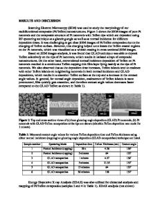
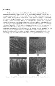
Fabrication of Crystalline Semiconductor Nanowires by Vapor-Liquid-Solid Glancing Angle Deposition (VLS-GLAD) Technique Arif S. Alagoz and Tansel Karabacak Department of Applied Science, University of Arkansas at Little Rock, Little Rock, AR 72204, U.S.A. ABSTRACT Vapor-liquid-solid (VLS) method has become one of the few and most powerful bottomup single crystal nanowire growth techniques in nanotechnology due to its easy scalability from micro to nano feature sizes, high throughput, relatively low cost, and its applicability to various semiconductor materials. On the other hand, control of growth direction and crystal orientation of nanowires, which determine their electrical, optical, and mechanical properties, stand as major issues in VLS technique. In this study, we demonstrate a new vapor-liquid-solid glancing angle deposition (VLS-GLAD) fabrication approach to produce crystalline semiconductor nanowires with controlled geometry. VLS-GLAD is a physical vapor deposition nanowire fabrication approach based on selective deposition of nanowire source atoms onto metal catalyst nanoislands placed on a crystal wafer. In this technique, collimated obliquely incident flux of source atoms selectively deposit on catalyst islands by using “shadowing effect”. Geometrical showing effect combined with conventional VLS growth mechanism leads to the growth of tilted crystalline semiconductor nanowire arrays. In this study, we report morphological and structural properties of tilted single crystal germanium nanowire arrays fabricated by utilizing a conventional thermal evaporation system. In addition to the tilted geometry, by introducing substrate rotation, nanowires with various morphologies including helical, zig-zag, or vertical shapes can be fabricated. Engineering crystalline nanowire morphology by using VLS-GLAD have the potential of enabling control of optical, electrical, and mechanical properties of these nanostructures leading to the development of novel 3D nano-devices. INTRODUCTION Nanotechnology is a rapidly expanding interdisciplinary field, promising novel devices for broad range of applications. Quantum effects and surface to volume ratio of nanostructures are strongly size dependent, and redefine material properties at nanoscale. Therefore enabling material fabrication and characterization techniques are critical for the development of nanodevices. Over the past decades, a vast amount of research work focused on controlled fabrication and characterization of 0D nanodots [1], 1D nanowires [2], and 2D layers [3]. On the other hand, fabrication of well controlled three-dimensional (3D) nanostructures in specific shape, size, and crystal structure is still a big challenge. About a half century ago, Wagner and Ellis demonstrated homoepitaxial growth of crystal silicon wires (or whiskers) by chemical vapor deposition (CVD) of silicon atoms through small droplets of metal catalyst [4-6]. They showed that at elevated temperatures metal-Si eutectic formation was followed by the growth of crystalline silicon wires and ca
Data Loading...