Fabrication of Mechanical Microstructures Using Amorphous Silicon Films on Glass Substrates
- PDF / 6,303,402 Bytes
- 6 Pages / 612 x 792 pts (letter) Page_size
- 25 Downloads / 336 Views
FABRICATION OF MECHANICAL MICROSTRUCTURES USING AMORPHOUS SILICON FILMS ON GLASS SUBSTRATES Chingwen Yeh, James B. Boyce, Jackson Ho, and Rachel Lau Xerox Palo Alto Research Center, 3333 Coyote Hill Road, Palo Alto, CA 94304 ABSTRACT A new process of surface micromachining has been developed, where amorphous silicon (aSi) and oxynitride films are used as structural and sacrificial layers on the glass substrate, respectively. Due to glass as the substrate material, the temperatures for all process steps need to be lower than 600°C. Some generic mechanical microstructures such as cantilever beams, bridges, and membranes have been fabricated. The stress changes of a-Si films with annealing temperatures are studied. It is found that the residual stress can be minimized using thermal annealing at 430°C for a few hours. In addition, some process issues such as a-Si film bubbling, the film adhesion of a-Si to the glass substrate, and stiction during structure release are discussed. INTRODUCTION MEMS (MicroElectroMechanical Systems) technologies have recently become very important in manufacturing various sensors and actuators for many applications, including avionics, biomedicine, data storage, environmental monitoring, space, transportation, and so on. However, using single-crystal silicon substrates is a significant limitation of these MEMS technologies for some applications, in which large-area substrates are required. Amorphous silicon on the glass substrate provides an approach to broaden MEMS technologies and brings them into the large-area applications. Unlike polycrystalline silicon, a-Si is usually deposited at lower temperatures (below 400°C) in PECVD (Plasma-Enhanced Chemical Vapor Deposition) systems, thus allowing the fabrication of microstructures on the glass substrate. In 1991, S. Chang [1] employed a-Si and aluminum films as structural and sacrificial layers on the silicon substrate, respectively. It was found that the residual stress of a-Si would depend upon the hydrogen content, which changed with annealing temperatures. More recently, it has been reported by M. Boucinha [2] that, using hydrogenated amorphous silicon (a-Si:H), mechanical microstructures can be made on the glass substrate, where the residual stress of aSi:H on the glass substrate has not been addressed yet. Here we present surface micromachining process of a-Si on the glass substrate and study the relation of the residual stress of a-Si with annealing temperatures.
A21.3.1
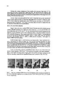
FABRICATION PROCESS Figure 1 illustrates the fabrication process flow. The process starts with Corning 1737 glass substrates. The first step is a-Si (0.3µm thick) and oxynitride (2µm thick) deposition using PECVD (Figure 1a). The a-Si and oxynitride films are used as a ground layer and a sacrificial layer, respectively. The ground layer can prevent the glass substrate from being attacked by BOE (Buffered Oxide Etchant) during microstructure releasing subsequently. The second step is patterning the sacrificial layer, where 6:1 BOE is used to etch the sacrificial layer
Data Loading...