Faceted growth of silicon crystals in Al-Si alloys
- PDF / 1,724,717 Bytes
- 11 Pages / 612 x 792 pts (letter) Page_size
- 95 Downloads / 289 Views
I.
INTRODUCTION
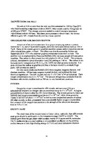
WHEN the primary silicon phase is precipitated from hypereutectic aluminum-silicon alloy melts, it forms as individual faceted crystals with a wide variety of morphologies, but with a strong trend toward predominance of octahedral crystals faced by {111} facets. {111} is the densely packed cleavage plane in the diamond cubic structure of silicon crystals. The growth of faceted crystals requires large supersaturation of the melt unless there is some geometrical factor that facilitates the formation of new atomic layers on a facet without the necessity of two-dimensional nucleation of each layer. Two such factors are known. One is the emergence of dislocations on the facet surface, which promote continuous spiral growth of successive atom layers.[1] The second is the twin plane re-entrant edge (TPRE) mechanism by which a stable groove maintained at the surface of a twinned crystal facilitates rapid growth in a specific direction, which is ^112& when the twinning plane is {111}, as in silicon[2]. Primary silicon octahedra are frequently twinned, to form spinel crystals (Figure 1), and they can nucleate and grow with very little undercooling below the silicon liquidus. There was therefore an early assumption that their growth was facilitated by the TPRE mechanism. The assumption was based on the known behavior of silicon in the Al-Si eutectic and strengthened by the occurrence of platelike primary silicon crystals, which were shown to grow by the TPRE mechanism.[4] However, closer examination of the twinned spinel crystals made it clear that the twins have little or no influence in their growth behavior.[5] More recently it has been proposed[6] that crystal growth in directions normal to the facets occurs by spiral growth around emerging dislocations. Dislocation-aided growth has been clearly demonstrated in experiments by Bauser and Strunk[7] on semiconductor grade silicon. A notable feature in the growth of faceted crystals is the appearance of striations resulting from the unloading of impurities across the facet planes at more or less regular inRU-YAO WANG, Professor, Department of Mechanical Engineering, and WEI-HUA LU, Senior Engineer, Department of Materials Engineering, are with the China Textile University, Shanghai 200051, People’s Republic of China. L.M. HOGAN, Hon. Research Associate, is with the Department of Mining and Metallurgical Engineering, The University of Queensland, Brisbane, Qld4072, Australia. Manuscript submitted February 6, 1996. METALLURGICAL AND MATERIALS TRANSACTIONS A
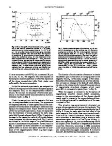
tervals. These impurity-rich layers mark the external shape of the crystal at stages during its growth, and their traces can be revealed by etching of metallographic sections.[7,8–10] In Figure 2, these ‘‘growth traces’’ appear as concentric lines parallel to external facets in a spinel-type crystal sectioned normal to the central twin plane. An important feature is that the spacing between successive traces varies for different facets. The spacing can thus be used to measure the variation in growth rate i
Data Loading...