Features of Semiconductors during Nanoindentation
- PDF / 166,859 Bytes
- 6 Pages / 595 x 842 pts (A4) Page_size
- 101 Downloads / 442 Views
W5.18.1
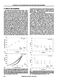
Features of Semiconductors during Nanoindentation Asta Richter 1, Bodo Wolf 1, Roger Smith 2 and Margita Günther 3 1: University of Applied Sciences Wildau, Bahnhofstrasse 1, D-15745 Wildau, GERMANY 2: Loughborough University, Loughborough, Leicestershire LE11 3TU, U. K. 3: Technical University Dresden, Department of Solid State Electronics, D-01062 Dresden, GERMANY ABSTRACT Si and InSb were subject to depth sensing multi-cycling nanoindentation. The load-depthcurves exhibited hysteresis loops which are explained in terms of pressure induced phase transformations. In order to study the impact of crystal distortions on phase transformation, the specimens were subject to boron implantation (ion energy 180 keV) of different implantation doses (1014 to 1017 ions/cm2) and indented without annealing. In InSb, the hysteresis loops disappeared after implantation of 1016 ions/cm2, and for Si with its stronger bonds, a dose of 3*1016/cm2 is required for the same effect. Indentation cycling with constant maximum load results in a sudden disappearance of the hysteresis loop after a small gradual loop area reduction during the first initial cycles. INTRODUCTION Indentation - static loading of a single hard asperity against the surface of the specimen – is one of the most widely spread techniques to determine mechanical properties of structured materials [1]. However, one has to take into account, that the three-dimensional stress field, and the inhomogeneous straining, resulting from indentation, complicate the interpretation of the measured data. Uniaxial compression and tension tests are much more suited to obtain quantitative information on the fundamental processes of plastic deformation. But these techniques will fail when inhomogeneous samples are addressed, and spatially resolved information is required. Furthermore, testing of very small samples proves also very complicated. A third point is, that mechanical properties are size dependent. Brittle materials, such as quasicrystals, ceramics and many semiconductors, are often completely destroyed when stress and strain in uniaxial deformation exceed the elastic limit. In contrast to this, they exhibit a certain ductility during small scale indentation. For these reasons, indentation testing – and nanoindentation in particular – plays an increasingly important role in mechanical characterization of novel materials, layer systems, and laterally structured objects, as electronic devices and micro-electromechanical devices [2]. Depth sensing nanoindentation provides much more information than the classical hardness measurement where the imprint is first generated, and later imaged using some microscopy. During depth sensing indentation the load F and the penetration depth h are recorded simultaneously, and the hardness H and the elastic modulus E are inferred from the resulting load-depth curve F(h). The standard technique of data analysis was established by Oliver and Pharr [3] but in addition, curve discontinuities, such as steps and slope changes, hint at certain ev
Data Loading...