Fluorine Atom Production Mechanisms From COF 2 and NF 3 in Uv Laser Etching of Poly-Silicon and Molybdenum
- PDF / 1,024,080 Bytes
- 9 Pages / 417.6 x 639 pts Page_size
- 55 Downloads / 273 Views
FLUORINE ATOM PRODUCTION MECHANISMS FROM COF 2 AND NF3 IN UV LASER ETCHING OF POLY-SILICON AND MOLYBDENUM
GARY L. LOPER AND MARTIN D. TABAT Chemistry and Physics Laboratory, 92957, Los Angeles, CA 90009
The
Aerospace Corporation,
P.
0. Box
ABSTRACT Ultraviolet laser-induced, radical-etching processes developed by us can provide practical etch rates and selectivities for most of the important film layer combinations used in silicon microelectronic devices. These processes have been demonstrated in simple proximity and projection exposure experiments to produce etch features on surfaces with dimensions of a few tenths of a micrometer. Mechanistic studies suggest that, in our etching processes for polysilicon and molybdenum, fluorine atoms responsible for etching are primarily produced from the precursors COF 2 and NF3 on the surface rather than in the gas phase. The predominant production process appears to be photodecomposition of surface adsorbed precursor. Contributions due to precursor pyrolysis or precursor reaction with photogenerated charge carriers are found to be unimportant.
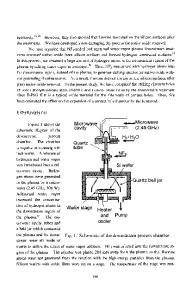
INTRODUCTION Integrated circuits are built up in multiple layers by successively depositing and then patterning and etching thin semiconductor, metal, and insulator film layers on a substrate. Because lasers can induce localized chemical reactions on surfaces, laser-induced chemical processes are being examined as methods to produce circuit patterns with submicrometer linewidths on these film layers during microelectronic device fabrication. Due to light diffraction effects, infrared and visible lasers cannot pattern surfaces with linewidths smaller than about lpm unless nonlinear chemical processes are employed. Ultraviolet (UV) laser-enhanced chemical processes thus are being primarily investigated for use in fabrication steps requiring submicrometer resolution. Much of the UV laser work is being directed at developing maskless etching processes [1-9]. We have developed maskless UV laser-induced radical-etching processes that can efficiently and selectively etch, with submicrometer resolution, most of the important film layer combinations used in silicon microelectronic devices [2,5,6,9]. By the laser etching technique, radical etchants are generated in the desired pattern at a gas/surface interface by UV laser-induced decomposition processes of precursor compounds. The surface may undergo etching reactions with these radicals. Surface material is removed by the formation of volatile compounds containing the surface elements. The proper selection of radicals allows the highly selective removal of the topmost film layer of a wafer relative to its underlying substrate. The technique allows the single step patterning and etching of surfaces. The method could greatly simplify the fabrication of submicrometer linewidth devices by eliminating photoresist patterning and acid or plasma etching processing steps. This paper briefly reviews our work toward developing UV laser radical etching processes for silicon device materials. The etc
Data Loading...