Focused ION Beam Etching of GaN
- PDF / 1,742,134 Bytes
- 6 Pages / 417.6 x 639 pts Page_size
- 30 Downloads / 478 Views
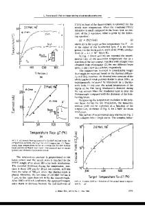
te this article as: MRS Internet J. Nitride Semicond. Res. 4S1, G6.57 ABSTRACT We have investigated the use of focused ion beam (FIB) etching for the fabrication of GaN-based devices. Although work has shown that conventional reactive ion etching (RME) is in most cases appropriate for the GaN device fabrication, the direct write facility of FIB etching - a well-established technique for optical mask repair and for IC failure analysis and repair - without the requirement for depositing an etch mask is invaluable. A gallium ion beam of about 20nm diameter was used to sputter GaN material. The etching rate depends linearly on the ion dose per area with a slope of 3.5x]0-4 m 3/pC. At a current of 3nA, for example, this corresponds to an etch rate of 1.05Pm 3/s. Good etching qualities have been achieved with a side wall roughness significantly below 0. 1pm. Changes in the roughness of the etched surface plane stay below 8nm. INTRODUCTION Tremendous effort has been made in recent years in developing GaN-based devices due to their wide spectrum of potential applications ranging from short-wavelength light emitters and lasers, solar-blind detectors to high temperature devices [1-4]. GaN-based devices reported to date have mostly been fabricated using reactive ion etching (RME) [5]. RIE-etched side walls, however, often suffer from a significant surface roughness, which is a major concern, e.g., for laser diodes since optical losses in the laser end mirrors increase the threshold current. Because of the difference in the cleavage plane between GaN (1100) and the commonly used sapphire substrate (1102) it is difficult to achieve flat cleaved end mirrors. The development of improved etching techniques is therefore essential to enhance the performance of GaN-based devices [68]. Furthermore, it will be necessary to find etching techniques which allow the fabrication of GaN on the nanometer scale for the development of novel device structures,, e.g., for integrating laser diodes with wavelength selective electro-absorbers [7]. Focused ion beam (FIB) etching is not only the most promising technique for the fine patterning of GaN-based devices, but also for improving the quality of laser facets. A focused gallium ion beam of 5-20nm size is used in FIB to sputter material. The direct write facility of focused ion beam (FIB) etching - a well-established technique for optical mask repair and for IC failure analysis and repair - without the requirement for depositing an etch mask is invaluable. This allows the nanometer scale fabrication of nitride devices. Focused ion beam (FIB) etching G 6.57 Mat. Res. Soc. Symp. Proc. Vol. 537 ©1999 Materials Research Society
has also great potential for the post-processing of devices and has been successfully applied to achieve polarization control in red GaAs-based vertical cavity surface emitting lasers (VCSELs) [9,10]. In this report, we determine basic parameters for the FIB-etching of GaN. We investigate the quality of FIB-etched GaN structures using atomic force microscopy and scanning elect
Data Loading...