Formation of Ni/Pt/Au Ohmic Contacts to p-GaN
- PDF / 1,030,339 Bytes
- 6 Pages / 414.72 x 648 pts Page_size
- 12 Downloads / 359 Views
Mat. Res. Soc. Symp. Proc. Vol. 482 0 1998 Materials Research Society
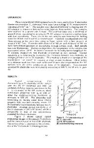
employed for p-ohmic contacts at 800 °C and 725 'C respectively, their specific contact resistance was 53 Qcm 2 for Au/p-GaN and 214 Qcm 2 for Au/Mg/Au/p-GaN respectively [11]. For the formation of low resistance p-GaN ohmic contacts, metal work functions should be about 7.5 eV to provide no offset at the interface [12]. Metal work functions should be much larger than that of GaN. However, metals with such a large work functions are not available. In this paper, a new Ni/Pt/Au trilayer metallization scheme is reported to achieve a low resistance p-GaN ohmic contact. EXPERIMENT Mg-doped GaN films were grown by metalorganic chemical vapor deposition (MOCVD). A 0.5 grn thick layer was grown on a 2.5 prm unintentionally doped GaN with a 50 ram AIN buffer layer over (0001) sapphire substrate. The doping concentration of p-GaN layer measured using Hall measurement was 9.4 x 1016 cm 3 . Prior to the photolithography, the samples were ultrasonically degreased with trichloroethylene (TCE), acetone, methanol, and deionized (DI) water for 5 min for each step. They were then patterned using a lithographic technique. The inner dot radius was 105 grm and the spacings between inner and outer circular dots were 3, 4, 6, 12, 13, 16, 21 trn. Prior to metal deposition, a buffered oxide etchant (BOE) was employed to remove the native oxide layer on GaN. The samples were then rinsed in DI water, blown by N 2, and immediately transferred into an electron-beam evaporator chamber. All metal thin films were deposited on the surface of GaN by an electron-beam evaporator under 1.5 x 10'6 torr base pressure. The deposition sequence was Ni / Pt / Au and with thicknesses of 20 / 30 / 80 nm. The metallization patterns were defined using a lift-off technique. A rapid thermal annealing (RTA) process in an Ar atmosphere was employed to find a good ohmic contact condition at temperatures varying from 300 "C to 850 "C. The current-voltage (I-V) data were measured with HP4155A and the specific contact resistance was calculated by the c-TLM method [ 13]. Auger electron spectroscopy (AES) depth profiles were performed to investigate the interfacial reactions between the metals and GaN. Atomic force microscope (AFM) was used to observe the surface morphology. RESULTS Fig. 1 shows the I-V characteristics of the Ni/Pt/Au contacts on p-GaN. The I-V data were measured by injecting currents up to ± 100 ýtA and by measuring the voltage across the circular contacts with a parameter analyzer, HP4155A. The as-deposited Ni/Pt/Au contacts on p-GaN exhibited near rectifying characteristic behavior. This is probably due to the formation of Schottky contact because work functions of metals used in this experiment are lower than that of p-GaN. When the contacts were annealed at 500 "C for 30 sec, the contact showed a linear behavior and the specific contact resistance was 2.1 x 10.2 Qcm2 . The specific contact resistance depends on the semiconductor sheet resistance [13]. Therefore, this specific c
Data Loading...