Functionalisation of Microfluidic Channels with In Situ Grown Carbon Nanotubes
- PDF / 773,869 Bytes
- 5 Pages / 612 x 792 pts (letter) Page_size
- 79 Downloads / 355 Views
J18.10.1
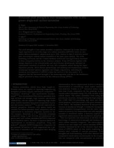
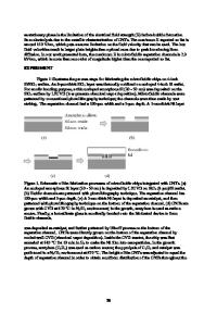
Functionalisation of Microfluidic Channels with In Situ Grown Carbon Nanotubes K. Gjerde1, T. Schurmann1, K.B.K. Teo2, M. Aono2, W.I. Milne2 and P. Bøggild1 1 NanoDTU, MIC - Dept. of Micro and Nanotechnology, Technical University of Denmark, Building 345 east, DK 2800 Kongens Lyngby, Denmark. 2 Dept. of Engineering, University of Cambridge, Trumpington Street, Cambridge CB2 1PZ, UK. ABSTRACT We present a new route towards customizing the surface properties of microfluidic channels, by a forest of in situ grown multiwalled carbon nanotubes (CNT). Local distortions of the electrical field direction are used to control the direction of the carbon nanotube growth. INTRODUCTION Carbon nanotubes have so far been proposed for a number of applications, some involving integration with Microsystems. So far, relatively few examples of carbon nanotubes directly synthesized on Microsystems are known. Recently, Carbon Nanotubes have been grown directly on AFM cantilevers for high aspect ratio tips [1]. In microfluidics, vertical forests of multiple carbon nanotubes could increase the surface area dramatically as well as function as nanoparticle filters. Here the inclination angle or growth direction of the carbon nanotubes may be an important parameter, as this could give rise to anisotropic properties, such as for instance a directional difference in the flow resistance. In the current work we used Plasma Enhanced Chemical Vapor Deposition (PECVD) to grow CNTs directly in microchannels etched in silicon by KOH. The CNT growth direction is guided by the electrical field [2-5]. Distortions of the electrical field allow us to control the inclination angle between the channel floor and the CNTs locally, and we demonstrate that simulations can be used to predict and design the geometry of field distorting structures. EXPERIMENTAL DETAILS We fabricated microliquid channels on Si (100) wafers by conventional photolithography and KOH etch using SiO2 as an etch mask. KOH etches silicon anisotropically, and with the etch rate in the (100) crystal direction of about 400 times the rate in the (111) direction, the resulting channels had flat floors with inclined sidewalls. An example of such a channel, with in situ grown CNTs is shown in figure 1. The channels varied in widths from 1 to 80 µm, and were etched to a depth of about 5 microns. The most narrow channels became more shallow due to the V-shaped profile resulting from the anisotropic KOH etch. PECVD grown nanotubes are grown from catalyst particles of transition metals such as Fe, Ni or Co. In this work we deposited a thin film of Ni inside the channels by a second lithography step, followed by metal deposition through electron beam evaporation and lift-off. Upon heating in the PECVD process, the film breaks up and agglomerates into catalyst particles. The average size of these catalyst particles can be controlled by the thickness of the deposited catalyst film, and since the diameter of the CNTs is controlled by the catalyst particle size, the average CNTs dimensions is in
Data Loading...