Gan Nucleation Mechanism on A Surface Template of Oxidized AIAs
- PDF / 4,066,974 Bytes
- 6 Pages / 414.72 x 648 pts Page_size
- 19 Downloads / 399 Views
Downloaded from https://www.cambridge.org/core. Columbia University Libraries, on 23 Jan 2020 at 14:24:10, subject to the Cambridge Core terms of use, available at https://www.cambridge.org/core/terms. https://doi.org/10.1557/PROC-512-47
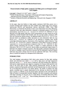
MOCVD. A two-step growth [6], optimized for this specific growth, was employed. Subsequently the AlAs layer was selectively oxidized in a gaseous mixture of H20/N2 at 425°C to form AIO,. Finally, the GaAs cap was removed to uncover the A1Ox surface. The AlAs in the other sample (denoted as sample B) was grown on Si(1 11) without a GaAs cap, thus oxidation proceeded through the AlAs surface. Two distinguishable A10. surfaces prepared in these ways were characterized by C-AFM and RHEED to examine microscopic surface morphology
Oxidation
"(11 J(bl
(a
(d7e)
Al (c~l
_I()
Fig. 1. Sample preparation procedure. (a)-(c) show sample A oxidized with
and crystallographic symmetry. After examination, both samples A and B were annealed at 1000*C in 02 ambient
GaAs cap. (d)-(f) show sample B
oxidized without GaAs cap.
before GaN was grown by atmospheric MOCVD using a closed-space shower head reactor. A multistep growth approach [7] that consists of multiple undoped GaN layers grown at successively higher temperatures was used to grow GaN, i.e. GaN-NL (-100A) was grown at 450°C followed by GaN buffer layer (-500A) at 800'C, then the 1St GaN overlayer (-1.5pJim) at 950 0C followed by the 2 nd GaN overlayer (-2.5pm) at 1000°C was grown. In another set of experiments, only a GaN-NL was grown on sample A and on an aA1203(0001) substrate. C-AFM and RHEED were used again to analyze microscopic surface morphology and crystallographic symmetry of GaN-NL. Furthermore, SAD and XTEM imaging were utilized to analyze crystallographic geometry and structural defects in the GaN overlayer on sample A by making a comparison with GaN on a-A20 3. RESULTS AND DISCUSSION As reported previously [5], single crystal ca-GaN showing macroscopically smooth surface morphology with a crystallographic orientation [000O1Ol]//[ I 1]si can be grown on sample A, while on sample B, a-GaN grows as randomly oriented large grains (diameter -4jim), resulting in extremely rough surface morphology. This naturally implies that the remarkable difference seen in the way ct-GaN evolves on sample A and B is most likely to be connected to the starting A10. surface preparation as mentioned in the previous section. Thus, we now focus on the A10. surfaces in sample A and B on which GaN growth is initiated. In Fig. 2, C-AFM images taken from as-formed AlOx surface in sample A and B are shown. Rectangular
domains dispersed evenly on the surface are apparent in (a). The rectangular domains have a lateral size of -4000A and average height variation is 81A, resulting in an r.m.s. roughness of 103A. In contrast to this, (b) shows indistinct morphology with no apparent surface feature Fig. 2. C-AFM images on (average height variation is 18A), leading to an r.m.s. AlO surface formed (a) with roughness of only 24A. Although C-AFM images are,
Data Loading...