Ge nanocrystals in MOS-memory structures produced by molecular-beam epitaxy and rapid-thermal processing
- PDF / 559,723 Bytes
- 5 Pages / 612 x 792 pts (letter) Page_size
- 44 Downloads / 300 Views
D6.2.1
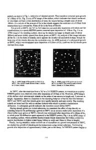
Ge nanocrystals in MOS-memory structures produced by molecular-beam epitaxy and rapid-thermal processing A.Nylandsted Larsen1, A. Kanjilal1, J. Lundsgaard Hansen1, P. Gaiduk1, P. Normand2, P. Dimitrakis2, D. Tsoukalas3, N. Cherkashin4, A. Claverie4 1 Institute of Physics and Astronomy, University of Aarhus, DK-8000 Aarhus C, Denmark 2 Institute of Microelectronics, NCSR Demokritos, 15310 Aghia Paraskevi, Greece 3 National Technical University Athens, School of Applied Sciences, 15780 Zografou, Greece 4 CEMES/CNRS, 29 rue J. Marvig, BP4347, F-31055, Toulouse, France ABSTRACT A method of forming a sheet of Ge nanocrystals in a SiO2 layer based on molecular beam epitaxy (MBE) and rapid thermal processing (RTP) is presented. The method takes advantage of the very high precision by which a very thin Ge layer can be deposited by MBE. With proper choice of process parameters the nanocrystal size can be varied between ~3 and ~8 nm and the area-density between ~1×10¹¹ and ~1×10¹² dots/cm2. The tunneling oxide thickness is determined by the thickness of a thermally grown SiO2 layer, and is typically 4 nm. C-V measurements of MOS capacitors reveal hole and electron injection from the substrate into the nanocrystals. Memory windows of about 0.2 and 0.5 V for gate-voltage sweeps of 3 and 6 V, respectively, are achieved. INTRODUCTION A considerable attention is presently focused on semiconductor nanocrystals (ncs) embedded into the silicon oxide of a MOSFET device for future high speed and low power consuming logic and memory devices [1], and a variety of fabrication procedures and structures are being tested [2-5]. The performance and the success of such a memory structure strongly depend on (a) the process ability for making uniform and reproducible thin tunnel oxides and (b) the characteristics of the islands (such as crystallinity, size, shape, orientation, spatial distribution) that influence both the potential energy of trapped electrons and the Coulomb blockade energy, which prevent the injection and storage of more electrons [6]. It has to our knowledge not yet been demonstrated whether Si or Ge is the better choice as the nanocrystal materials in such memory devices. It is, nevertheless, clear that differences in electronic structure, melting temperatures, diffusivity, solubility etc. between Si and Ge will influence the memory characteristics and the dot-formation kinetics. There are experimental indications for ion-beam synthesized nanocrystals that, in that particular case, nanocrystals of Si are to be preferred [7]. We have recently developed a procedure for the fabrication of a MOS device with embedded Ge ncs based on molecular beam epitaxy (MBE) in conjunction with rapid thermal processing (RTP). The reproducibility and the precision of this fabrication technique for the production of a layer of spherical, well-separated and crystalline Ge nanodots in a SiO2 layer suggest that this method could be widely applicable for the fabrication of memory devices. The method has been previously presented in Refs.8-10,
Data Loading...