Gettering of Impurities by Incoherent Light Annealed Porous Silicon
- PDF / 326,297 Bytes
- 5 Pages / 420.48 x 639 pts Page_size
- 95 Downloads / 353 Views
GETTERING OF IMPURITIES BY INCOHERENT LIGHT ANNEALED POROUS SILICON V. E. BORISENKO, A. M. DOROFEEV Minsk Radioengineering Institute, P.Browka 6, Minsk,
USSR
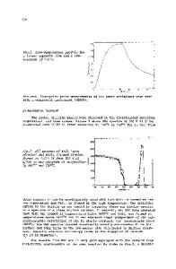
ABSTRACT The application of electrochemically formed porous silicon to getter Cu and Au atoms in silicon crystals during incoherent light annealing for 4 to 20 sec is r~ported. Exposure light power density of 30 W/cmL was used to heat the samples up to 950 °C. Improvement of lifetime related to Au and Cu gettering with porous silicon has been observed. Excess impurity interstitials and their enhanced diffusion are supposed to be responsible for the gettering effect. INTRODUCTION Heavy-metal impurities introduce energy levels within the bandgap of silicon, which act as a recombination centers, thus decreasing the minority carrier lifetime and increasing the leakage currents of p-n junctions [11. Gettering appears to be the only manner in which an appropriate yield of high quality devices can be achieved. Various techniques involving formation of damaged lattice regions or layers with enlarged intrinsic surfaces acting as a condensation sites for metallic contaminations and stacking fault nuclei have been presented to getter unwanted impurities in silicon [2]. Highly activated silicon surface can be provided with porous silicon fabricated by anodic treatment of silicon crystal in HF [3,4]. In order for gettering to occur, long-time high temperature heating is necessary for migration of impurities and their accumulation in a getter. Annealing temperatures ranged from 800 to 1200 °C and annealing cycles of 30 min and longer are inevitably employed [5-73. Meanwhile, there has been a growing interest in the application of short-time heat processing by intense incoherent light which has been succesfully used to anneal ion-implanted silicon [8-13]. In the present study electrochemically formed porous silicon layer has been used to getter heavy-metal impurities extracted out of a silicon crystal during rapid incoherent light annealing. EXPERINIENTAL The experimental arrangement is schematically shown in Fig.1. Structure of the sample, initial metal impurity profile and theoretically estimated impurity redistribution due to their gettering by the porous silicon layer are presented. Mat. Res.
Soc. Symp. Proc. Vol. 13 (1983) QElsevier Science Publishing Co.,
Inc.
376
I I I ILight iI I I
N
n-Si Annealed
IInitial
p-Si substrate
Porous Si
Cross section of the sample Fig.1.
xI
Metal impurity distribution
Schematic view of the experimental arrangement.
Substrates were 0,1 Ohm-cm p-type (111) silicon wafers of 380 1 um-thick and 76 mm in diameter. As a first step in a sample preparation, 2,0 m-thick n-epitaxial layer was formed at the front side of wafpers for lifetime measurements. The samples were unlgormly1aturated 3 with Au or Cu up to the concentrations of 10r - 10 atom/cm and chemically etched to remove impurity enreached surface layers. Porous silicon layer of 8-10_# m-thick was formed in a half of the silicon wafer back side by anodic dissolution in HF
Data Loading...