Grain Boundary Phase Analysis of Silicon Nitride by a Newly Developed 300kV Field-Emission Electron Microscope
- PDF / 3,299,225 Bytes
- 6 Pages / 414.72 x 648 pts Page_size
- 37 Downloads / 328 Views
In the present paper, the grain boundary phases of silicon nitride containing 1 mol% and 10 mol% of equi-molar additives Y 20 3 and Nd 20 3 are investigated by a 300kV FE-ATEM. It is shown that the compositions of the grain boundary phases between the two-grain boundary and the triple points are not the same. 2. EXPERIMENTAL PROCEDURE Silicon nitride powders (Starch, Hi grade) are mixed with sintering additives of 1 733 Mat. Res. Soc. Symp. Proc. Vol. 346. 01994 Materials Research Society
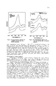
Fig.1 A minimum probe size of a 300kV FE-ATEM newly developed. The half-width of the minimum probe size is about 0.4 nm. mol% and 10 mol% of equi-molar of Y20 3 and Nd 2O3, which are named here as the sample SNI and SNIO in this paper. Then the powders are hot-pressed at 1900 0C for 4 hrs under a N2 gas in the pressure of 10Mpa8). The average particle sizes are about 0.6 um and they contain impurities of 0.43 wt% carbon and 1.37 wt% oxygen. Thin sections for ATEM observations are prepared by ion milling using Ar ions. The specimen are coated by carbon films to decrease charging up of the electron
beam.
a
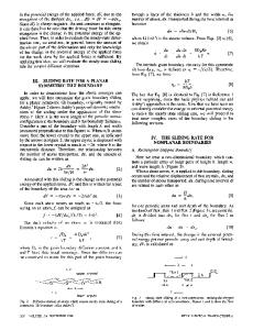
Fig.2 The microstructures of silicon nitride ceramics containing 1 mol% (SN1) (a) and 10 mol% (SN10) (b) of equi-molar of Y203 and Nd 2O3 additives.
734
The specimens are then observed by a newly developed 300kV FE-ATEM. The probe diameter of about 0.5 nm for the routine analysis at 300 kV is used as shown in Figure 1. The emission current of such a small prove is about 0.1 nA, which is enough to obtain sufficient x-ray signals. The energy dispersive x-ray spectra (EDS) are obtained when the fine electron beam is placed on the specimen area. The acquisition time is from 10 to 30 seconds. The x-ray solid angle is 0.20 str. for an ultra-thin window type x-ray detector with a take-off angle of 26 degree. 3. RESULTS AND DISCUSSIONS
Figure 2 (a) and (b) show low magnification images of the grain boundary structures of the samples SNI and SN10, respectively. Both specimens represent similar features of the microstructures, where the hexagonal-shaped matrix grains of about a few micron size are fully covered with the grain boundary phases having a dark contrast. These grain boundary phases are assigned as an amorphous structure from electron diffraction patterns. The triangular shapes of the boundary phases of the SN1O, located at the triple points are more thicker than those of the SNi, indicating the presence of the large amounts of the secondary glassy phases. It is also observed in the SN1O that large glassy pockets having a few micron size are formed among the matrix grains. In order to determine the thickness of the intergranular phase of the two-grain boundary, the high resolution images of the edge-on boundaries for the SNI and SN1O are observed and shown in Figure 3 (a) and (b), respectively. The intergranular amorphous thin films are clearly observed in both specimens. The thickness of the
intergranular films for the SNI is assigned to be about I nm, which is almost the same as those of the SN10. This means that the t
Data Loading...