Growth from Solution, Structure, and Optical Properties of Single-Crystal para -Quaterphenyl Films
- PDF / 1,242,770 Bytes
- 10 Pages / 612 x 792 pts (letter) Page_size
- 15 Downloads / 289 Views
TAL GROWTH
Growth from Solution, Structure, and Optical Properties of Single-Crystal para-Quaterphenyl Films V. A. Postnikova,*, N. I. Sorokinaa, O. A. Alekseevaa, V. V. Grebeneva, M. S. Lyasnikovaa, O. V. Borshchevb, N. M. Surinb, E. A. Svidchenkob, S. A. Ponomarenkob, and A. E. Voloshina a
Shubnikov Institute of Crystallography, Federal Scientific Research Centre “Crystallography and Photonics,” Russian Academy of Sciences, Moscow, 119333 Russia b Enikolopov Institute of Synthetic Polymeric Materials, Russian Academy of Sciences, Moscow, 117393 Russia *e-mail: [email protected] Received April 20, 2017
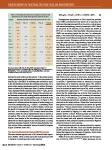
Abstract—Samples of single-crystal para-quaterphenyl films up to 8 mm long and 50 μm thick have been obtained for the first time by the solvent‒antisolvent growth method. The films have been grown both on the liquid–air interface and in the solution bulk. The morphology, surface quality, and thickness of crystal films have been investigated by the optical, laser confocal, and atomic force microscopies. The structure of the para-quaterphenyl single crystal at room temperature has been refined by X-ray diffraction analysis. The formation and growth mechanisms of crystal films on the liquid–air interface have been discussed. The opticalabsorption and photoluminescence spectra of the solutions and crystal samples have been investigated. DOI: 10.1134/S1063774518010157
INTRODUCTION Among various families of semiconductor organic oligomers, linear oligophenyls (р-nP, where n ≥ 4 is the number of phenyl rings in the molecular structure) are known as highly stable [1] blue light emitters with a high quantum photoluminescence yield [2, 3]. According to the data in the literature, vacuum thermal deposition on substrates is currently the main method for growing oligophenyl-based crystal structures for optoelectronics [4–6]. In particular, the development of a LED based on a vacuum-deposited para-sexiphenyl (р-6P) polycrystal layer was reported in [7]. The concept of a new light-emitting device was proposed quite recently; it is a light-emitting transistor (LET) [8] with a structure close to that of field transistor. A LET is considered as a promising device combining two functions: current control and light emission (when a conventional LED is used as a screen pixel, it requires an additional control transistor). The LET design is based mainly on the preliminary analysis of the field-transistor operation. It was reported in [9] that the hole mobility in the structures of field transistors based on vacuum-deposited polycrystalline layers of р-4P, р-5P, and р-6P oligophenyls reached 10–2–10–1 cm2/(V s) [9]. It is reasonable to suggest that the use of a single-crystal film with a low content of defects as an active layer will make it possible to develop a device with significantly improved electric transport characteristics, on the basis of which electroluminescence can be successfully realized.
Concerning the relative simplicity of realization, the deposition of thin crystalline layers directly on a substrate using growth from
Data Loading...