High Power SiC MESFETs
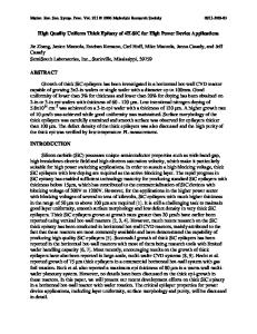
- PDF / 109,830 Bytes
- 5 Pages / 612 x 792 pts (letter) Page_size
- 82 Downloads / 336 Views
0911-B10-14
High Power SiC MESFETs Christopher Ian Harris1, Andrei O Konstantinov2, Jan-Olov Svedberg2, Ian Ray2, and Christer Hallin1 1 INTRINSIC Semiconductor Corp., 22660 Executive Drive, Dulles, VA, 20166 2 INTRINSIC Semiconductor AB, Osterogatan 3, Kista, 164 40, Sweden
ABSTRACT Results of the development of high power, high efficiency silicon carbide RF MESFETs are reported. High power densities of over 3W/mm have been measured for devices with total power output in excess of 20W. The devices have been fabricated using a novel lateral epitaxy technique. The MESFET employs a buried p-type depletion stopper in order to suppress short channel effects and increase the operation voltage. The use of the depletion stopper also allows high RF signal gain, while maintaining high voltage operation capability. High breakdown voltages of over 200 Volts are achieved for single-cell components; however large-area transistors are limited to around 150 Volts. Single-cell components measured on-wafer demonstrate an Ft of 10 GHz and a high unilateral gain. Packaged 6-mm RF transistors have been evaluated using amplifier circuits designed for operation in classes A, AB or C. Operation in class AB demonstrated a saturated power of 20 W and a P1dB of 15W with a linear gain of over 16 dB at Vdd of 60 V for 2.25 GHz operation. Maximum drain efficiency is 56% for class AB operation, 48% at 1 dB compression point and 72% for class C at 2.25 GHz. Preliminary linearity measurements have been performed using a two-tone technique. IM3 values of less than -40 dBc can be achieved even at relatively high power levels. INTRODUCTION The increasing maturity of Silicon Carbide technologies has meant that a range of semiconductor devices are now becoming available on the open market. SiC based MESFET devices are also available, however, there remains significant development work to demonstrate the potential of these devices for very high power operation. In order to optimize the performance of SiC devices the device technology needs to be adapted to make use of the unique capabilities of this material. In particular the high voltage capability requires a design that avoids short-channel effects (early ‘turn-on’ of the transistor at high drain bias). A novel design incorporating a buried p-type depletion stopper that prevent short channel effects has previously been proposed and demonstrated by the authors [1]. The development of this technology towards a commercial product has been on-going; in this paper we report the performance of state of the art SiC MESFETs and discuss some of the novel technologies incorporated in their manufacture.
EXPERIMENT Device Process A schematic of the SiC MESFET device discussed in this paper is shown in Figure.1; it is immediate apparent that in cross section the device resembles a traditional Silicon LDMOS. The LDMOS device is seen as a bench-mark for performance and indeed it is possible to apply much of the technology developed for LDMOS to it’s SiC cousin. The manufacture of the SiC device is however quite
Data Loading...