High Quality GaAs Mis Diodes With Very Low Surface State Density
- PDF / 250,087 Bytes
- 4 Pages / 420.48 x 639 pts Page_size
- 6 Downloads / 283 Views
HIGH
QUALITY GaAs MIS DIODES WITH VERY LOW SURFACE
STATE DENSITY
YOSHIHISA SUMIKO Research SAKAI*, SABURO ATAKA*, 1-280 AND KENJI SHIBATA* *Hitachi FUJISAKI*, Ltd., Central Laboratory, Higashikoigakubo, Kokubunji, Tokyo 185, Japan **Babcock-Hitachi K.K., Yokohama Research Lab., Yokohama, Kanagawa, Japan
ABSTRACT High quality GeAs/Si0 2 MIS( Metal Insulator Semiconductor ) diodes were fabricated using (NH4 ) 2 S treatment and photo-assisted CVD( Chemical Vapor Deposition ). The density of states at the GaAs and Si0 2 interface is the order of lol1 cm- 2 eV- 1 throughout the forbidden energy range, which is smaller by the order of two than that of the MIS devices made by the conventional CVD process. The mechanism attributable to the interface improvement was investigated through XPS( X-ray Photoelectron Spectroscopy ) analyses. INTRODUCTION
Recently, sulfur passivation of GaAs crystals has received a great attention since it improves the quality of GaAs surfaces. It is thought to be attributed to the termination of dangling bonds on the surface by sulfur atoms [1],[2],[3]. Though the detailed atomic scale structure of this sulfur passivated surface is not revealed yet, we can utilize this technique to reduce a surface state density of compound semiconductors. However, sulfur passivation does not last for long and requires some permanent protection above the treated surface [1],[4]. According to the study done by J.F.Fan et al [5], the formation of a permanent film on the (NH4 ) 2 S treated GaAs should be carried out very carefully since the treated surface suffers damage quite easily. In this report, we propose a new photo-assisted CVD process to compose a insulating Si0 2 film on a (NH4 ) 2 S treated GaAs surface. Due to a low damage feature of a photo-CVD process, we have succeeded in reducing the surface 2 1 state density down to the order of 101l cm- eV- . EXPERIMENTS The n type GaAs crystals were at first etched with 4H 2 SO4 /H 2 0 2 /H 2 0 solution for a few seconds to remove a damaged (NH in
4
layer. Then ) 2 S solution
Au
density.
order
to avoid
the thermal
'4 -(NH4)2S
After the
(NH4 ) 2 S treatment, wafers were loaded in a photo-CVD vacuum chamber. The chamber was once pumped up to i0-7 Torr to evacuate adsorped water, oxygen etc.. In damage
02
pliotoCVD Si02
minutes to get a quasi-ideal surface with low defect
TCVDVDSF02 Si
---
they were immersed at 50C for 10
Treated
Interface
n-GaAs i.
of
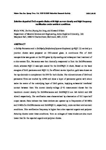
wafers, source gases were introduced AuGe(Ohmic) before the wafers were heated or irradiated by a ultra-violet light Fig. 1 Cross sectional view of a source. The sources for Si0 2 deposition MIS diode. were oxygen and SiH4 buffered with nitrogen. The total pressure and the pressure ratio between oxygen and SiH4 were set to be 9 mTorr and 10, respectively. The temperature of a wafer was varied from 200C to 300C. Mat. Res. Soc. Symp. Proc. Vol. 209. 01991 Materials Research Society
704
After the Si0 2 deposition, wafers were annealed at 350C for 1 hour in a pure hydrogen atmosphere to improve
Data Loading...