High Resolution Electron Microscopy of Sputter-Deposited Zirconia-Alumina Nanolaminates
- PDF / 3,347,862 Bytes
- 5 Pages / 414.72 x 648 pts Page_size
- 42 Downloads / 322 Views
Mat. Res. Soc. Symp. Proc. Vol. 403 ©1996Materials Research Society
Table I. Growth Architecture of Zirconia and Zirconia/Alumina Nanolaminates Number of A120 3 Layer ZrO2 Layer ZrO2 / A120 3 Thickness [nm] Thickness [nm] Layers Film 6, 9, 12.5, 17.5, 23, 35
10
A
6/5
B C
6/ 5 1/0
35, 23, 17.5, 12.5, 9, 6 110
10
D
1/0
20x4.5=90
-
HREM was performed on all films A, B, C, and D in a Hitachi H-9000NAR transmission electron microscope (TEM) operated at 300 kV. Cross-sectional TEM samples were prepared by mechanical polishing, dimpling, and Ar+ ion milling. High resolution lattice images were recorded directly using a retractable multi-scan CCD camera by Gatan. Accurate lattice spacing measurements were made from selections of the digital images by calculating numerical diffractograms of individual nanocrystallite regions using the Hanning window method [6]. RESULTS AND DISCUSSION Zirconia-alumina nanolaminate
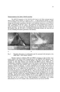
morphology:, Figure 1 shows a low magnification HREM image of film A illustrating the overall nanolaminate structure. The alumina layers, appearing lighter in the image, clearly separate the polycrystalline zirconia layers of different thicknesses. The first two zirconia layers (6 and 9 nm thick) were straight and had abrupt interfaces with the silica substrate and adjacent alumina layers. Higher magnification images (not presented here) showed zirconia nanocrystallites in the 6 and 9 nm layers to be slightly rounded and block-like in shape. The nanocrystallite
dimensions perpendicular to the substrate were, without exception, equal to the layer thickness. This result is consistent with previous XRD data for nanolaminates of comparable thickness [5] and HREM observations from a nanolaminate with 4.5 nm zirconia layers [7]. HREM imaging of the thicker (12.535 nm) zirconia layers showed a complex nanocrystalline structure associated, in part, with the growth transformation of t -> m-ZrO2. Furthermore, a roughness to the overall nanolaminate structure developed away from the substrate. It can be seen from Figure 1 that starting with the third zirconia layer (12.5 nm thick), a roughness to the layer structure developed that was more pronounced as the zirconia layer thickness increased. HREM imaging of these thicker zirconia layers showed that zirconia nanocrystallites renucleated within the zirconia layers during growth,
Figure 1: Transmission electron micrograph of film A imaged in crosssection. Zirconia layers appear dark in this image; alumina layers appear light.
Zirconia layer thicknesses [nm] are indicated along right hand side of image. 298
contributing to the layer roughness. The renucleation behavior of the zirconia nanocrystallites showed random orientation relationships to neighboring nanocrystallites, a further complication to the nanocrystallite structure of these thicker layers. Figure 2 is an HREM image typical of the 12.5 nm zirconia layer of film A. This image shows the renucleation of a zirconia nanocrystallite that occurred during growth of this layer and is representative of renu
Data Loading...