High Resolution UHV Electron Microscopy on Surfaces and Heteroepitaxy
- PDF / 3,260,107 Bytes
- 8 Pages / 420.48 x 639 pts Page_size
- 71 Downloads / 433 Views
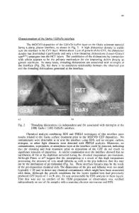
HIGH RESOLUTION UHV ELECTRON MICROSCOPY ON SURFACES AND HETEROEPITAXY K.TAKAYANAGI, Y.TANISHIRO, K.MUROOKA AND M.MITOME Tokyo Institute of Technology, Graduate School at Nagatsuta, Materials Science and Engineering, 4259 Nagatsuta, Midoriku, Yokohama, Japan 227. *Tokyo Institute of Technology, Physics Department, Ohokayama, Meguroku, Tokyo, Japan 152. ABSTRACT Surface structure observations by high-resolution UHV electron microscopy at the atomic level summarized. Both the profile imaging in transmission electron microscopy and superlattice imaging in reflection electron microscopy are applied to image the reconstructed structure of gold surfaces and Si(lll)7x7 surfaces. INTRODUCTION For atomic level imaging of surfaces and interfaces, profile imaging is widely used as demonstrated first[l] by the imaging of Au(ll0)2xl reconstructed surfaces[21. The high resolution microscopes ordinary used, however, do not enable us to study clean surfaces and dynamic processes due to the lack of ultra-high vacuum conditions and "in-situ" facilities such as evaporators. High resolution "in-situ" electron microscopy under UHV conditions to study clean and welldefined surfaces [3,4] was achieved rather recently in transmission electron microscopy (TEM) [5-7] and in reflection electron microscopy (REM)[7,8]. In addition to surface studies, high resolution electron microscopy has been used for the microclusters by Iijima and Ichihashi[9] and is expected as a new method of exploring the structure and dynamics of the microclusters. In this paper some of our recent observations using the high resolution UHV electron microscopy on reconstructed surfaces, microclusters and/or ultra-thin film growth are summarized. HIGH RESOLUTION UHV ELECTRON MICROSCOPE A high resolution UHV electron microscope of 200 kV acceleration (JEM 2000FXV) was designed [5,7] to achieve 0.21 nm point-to-point resolution, 10 Torr vacuum and "in-situ" capability in TEM and REM. Fig.1 shows a view of the microscope: a are evaporators; @ is a heat conductor for a anti-contamination shroud surrounding the specimen; © is the side entry specimen holder and gonlometer, and •dis the objective aperture control. Each of the evaporators is now redesigned to be exchangeable through a gate valve and a gasinlet system is attached at the port @. As described previously, the construction of the objective pole-piece around the specimen enables observations of the lateral surface of the specimen by the profile TEM imaging or REM. The SI(lll) and (001) specimens for REM study were 6mmxlmmxO.2mm and are cleaned by passing electric current Mat. Res. Soc. Symp. Proc. Vol. 139. -1989 Materials Research Society
60
Fig.1
High resolution UHV electron microscope (JEM2000FXV). Construction around the specimen chamber for "in-situ" surface strudy at atomic resolution.
through the specimen. The temperature of the specimen surface is monitored by the current. The graphitized carbon films are used as the substrate for the Au deposition to observe the growth of Au clusters and Au surfaces by pr
Data Loading...