High Resolution XRD Studies of Ion Beam Irradiated InGaAs/InP Multi Quantum Wells
- PDF / 190,051 Bytes
- 8 Pages / 612 x 792 pts (letter) Page_size
- 81 Downloads / 244 Views
1020-GG07-24
High Resolution XRD Studies of Ion Beam Irradiated InGaAs/InP Multi Quantum Wells Dhamodaran S1, Sathish N1, Anand P Pathak1, Andrzej Turos2, Devesh K Avasthi3, and Brij M Arora4 1 School of Physics, University of Hyderabad, Central University (P.O), Hyderabad, 500 046, India 2 Institute of Electronic Materials Technology, Warsaw, 01-919, Poland 3 Inter University Accelerator Centre, New Delhi, 110 057, India 4 Tata Institutte of Fundamental Research, Mumbai, 400 005, India
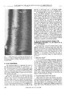
ABSTRACT To investigate the interface modifications of multi quantum wells InGaAs/InP grown by metal organic chemical vapor deposition have been irradiated using swift heavy ions. Irradiation has been performed using 150 MeV Ag12+ and 200 MeV Au13+ ions. Both as-grown and irradiated samples were subjected to rapid thermal annealing at 500 and 7000C for 60s. Asgrown, irradiated and annealed samples were subjected to high resolution x-ray diffraction studies. Both symmetric and asymmetric scans were analyzed. The as-grown and Ag ion irradiated samples show sharp and highly ordered satellite peaks whereas, the Au ion irradiated samples show broad and low intense peaks. The higher order satellite peaks of the annealed samples vanished with increase of annealing temperature from 500 to 7000C, indicating mixing induced interfacial disorder. Annealing of irradiated samples show higher mixing and disorder and no higher order satellite peaks were observed. In comparison with as-grown samples no strain was observed after high temperature annealing of as-grown samples. Strain values calculated from the X-ray studies indicate that the irradiated samples have higher strain 0.2041% which has been reduced as a function of annealing as 0.1704% and 0.1509%. This indicates that the annealing induced mixing occurs maintaining the lattice parameter close to that of the substrate. In similar samples such results have been observed and reported in literature. The effect of electronic energy loss for interface mixing has been discussed in detail. The role of incident ion fluence in combination with the electronic energy loss has also been discussed.
INTRODUCTION Growth of InGaAs/InP using various epitaxial techniques has been reported. To date, the material that has been used most widely as an absorber is In0.53Ga0.47As. The two important characteristics that contribute to the use of this alloy are that (i) it exhibits strong photoresponse in the wavelength range from 1.0 to 1.6µm and (ii) high quality, lattice matched epitaxial layers can be grown on InP. The stability of such heterostructures is important from the device performance point of view. The composition and layer thickness are the parameters used to tune various physical properties. Apart from the lattice matched composition, strain heterostructures of InGaAs/InP are also useful in several applications. In strained heterostructures critical layer thickness is important since beyond this critical thickness defects are generated which deteriorate the device performance. Critical layer thicknes
Data Loading...