High Resolution Z-Contrast Imaging of Semiconductor Interfaces
- PDF / 3,690,387 Bytes
- 7 Pages / 604.8 x 806.4 pts Page_size
- 94 Downloads / 353 Views
Defocus (Â) -500
-600
-700
-800
-900
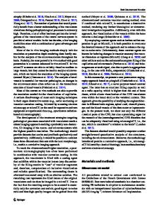
Figure 1. Montage of phase contrast simulated images for Si(110). The accelerating voltage is 400 keV, and the objective lens spherical aberration coefficient Cs is 1 mm (Scherzer resolution limit 1.7 A).
Introduction The structural and compositional integrity of interfaces between semiconductor multilayers can profoundly influence the optical and electronic properties of
34
epitaxially grown heterostructures. Understanding the atomic-scale interfacial structure and chemistry is therefore essential to correctly relate electrical measurements to theoretical models and to
correlate such effects with growth conditions. High-resolution électron microscopy (HREM) has played a pivotai rôle in this process, providing important information on interface commensurability and revealing the présence and nature of defects. More recently, significant advances hâve been made in applying HREM to the difficult problem of chemical composition m a p p i n g in Systems w h e r e no structural change occurs across the interfaces. 1 The basis of such methods involves using the objective lens as a bandpass filter and tuning in on a spécifie range of spatial frequencies to form a chemically sensitive interférence pattern. By using a suitable low-index zone axis and choosing an optimum range of spécimen thickness, the p a t t e r n s can indeed be extremely sensitive to the strength and periodicities of the projected potential. However, the results also dépend critically on other expérimental parameters including small spécimen tilts and strains. It is customary to establish the optimum expérimental chemical mapping conditions from a séquence of image simulations based on the anticipated structure and chemistry of the System under investigation. This type of pretuning may, however, reduce the sensitivity of the interférence pattern to unforeseen structural effects, which might easily be overlooked in the image. This article présents a new strategy for compositional mapping at semiconductor interfaces, using Z-contrast scanning transmission électron microscopy (STEM). Our approach is to incoherently image an interface object function which is intuitively related to the structure and chemistry of the interface. Images exhibit a weak thickness dependence and a strong (Z2) chemical sensitivity. No pretuning of the expérimental conditions is required since the instrument is operated at standard defocus conditions for ail spécimens. This direct method provides the crystal grower with immédiate feedback on the atomic-scale structure and chemistry of the heterostructure, and most importantly, rapidly identifies unexpected effects. We illustrate thèse points through expérimental studies of ultrathin (Si m Ge n ) p superlattices and CoSi2/Si interfaces which demonstrate the unique insights the technique can provide into the atomistic processes occurring during epitaxial growth. H o w to Think A b o u t Z-Contrast Images Z-contrast STEM imaging is funda-
MRS BULLETIN/MARCH1991
High Resolution Z-Contras
Data Loading...