Identification of Surface-Related Electron Traps in Undoped GaAs by Deep Level Transient Spectroscopy
- PDF / 172,275 Bytes
- 4 Pages / 420.48 x 639 pts Page_size
- 61 Downloads / 322 Views
IDENTIFICATION OF SURFACE-RELATED ELECTRON TRAPS IN UNDOPED GAAS BY DEEP LEVEL TRANSIENT SPECTROSCOPY KI-CHUL SHIN AND IN-SHIK PARK GoldStar Cable Research Lab., 555 Hogye, 430-080
Anyang,
Kyungki,
Korea,
ABSTRACT Using undoped GaAs containing grain boundary, we performed annealing test to identify the processes occurring during heat treatment. We propose EL2 as a complex of double vacancy, Asca From the concentration change at grain boundary region and Asi . we temporarily conclude that EL3 is a simple intrinsic defect. INTRODUCTION In the processing of GaAs device, it is important to understand the nature of defects present to make best use of them or to get rid of them, if possible. The most dominantly found defect,EL2, has been studied very extensively, but the origin of it is not clear yet. Also the origin of EL3 level which is said to be related with the surface damage [11 is not verified. It is well known that grain boundary in semiconductors works as a potential barrier. In the measurement of DLTS, this barrier has been used insteadof surface Schottky barrier to study grain boundary region in GaAs [2]. Since a grain boundary acts as a sink for point or line defects, the annealing behavior of defects can easily be seen near grain boundary and this can be used to understand the annealing mechanism and the composition of
deep level defects
in
GaAs.
EXPERIMENT
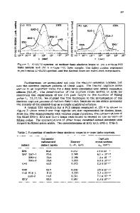
Samples were cut from horizontal Bridgman (HB) grown undoped GaAs crystal which is slightly As-rich. Measured carrier concentration was 6 x 10¹⁶ /cm 3 , n-type. Sample was chosen such that grain boundary runs through the middle of the sample with size of 8 x 1.2 mm. Sample thickness was 420 dm. Annealing was performed at 200*C, 350*C, and 500 0 C for one hour in the flowing small argon gas. Ohmic contacts were prepared by evaporating dots of Au:Ge. DLTS measurement was done with Bio-Rad model number DL4600. RESULTS AND DISCUSSION Peak intensity change due to annealing Figure 1 shows DLTS peak intensity change of observed traps in undoped GaAs grain sample for different annealing temperatures. According to Dannefear et al's positron annihilation experiment (3], the most dominant point defect in undoped GaAs is double vacancy (VGaVAs) which anneals at 350°C - 4000C. Theref0 ore, in samples annealed below 350 C (hereafter called stage A anneal), point defects consist mostly of double vacancies, and in samples annealed at or above 350°C (hereafter called stage B Mat. Res. Soc. Symp. Proc. Vol. 163. 1990 Materials Research Society
212
n
x3
EL2
z z -J
0I
EL3 L
0
Fig.
200 350 Annealing temperature (C
500
1 Peak intensity change after annealing
anneal), double vacancy is no more prevailing species and single vacancy-related defect (VaA• ) is the dominant one. From this argument, Wager et al 14] proposed that EL2 is a double vacancyrelated defect (VG ASGaVa or VAsVGaAsa) and that EL2 forms a group of family. Ko explain the outdiffusion of EL2 under annealing, Min et al [5] syggested VAsAsi VGaAs•a to be a plausible model for EL2 on the basis
Data Loading...


